SBASAF4 September   2021 TMAG5170

PRODUCTION DATA  

  1. Features
  2. Applications
  3. Description
  4. Revision History
  5. Pin Configuration and Functions
  6. Specifications
    1. 6.1 Absolute Maximum Ratings
    2. 6.2 ESD Ratings
    3. 6.3 Recommended Operating Conditions
    4. 6.4 Thermal Information
    5. 6.5 Electrical Characteristics
    6. 6.6 Magnetic Characteristics
    7. 6.7 Power up Timing
    8. 6.8 SPI Interface Timing
    9. 6.9 Typical Characteristics
  7. Detailed Description
    1. 7.1 Overview
    2. 7.2 Functional Block Diagram
    3. 7.3 Feature Description
      1. 7.3.1 Magnetic Flux Direction
      2. 7.3.2 Sensor Location
      3. 7.3.3 Magnetic Range Selection
      4. 7.3.4 Update Rate Settings
      5. 7.3.5 ALERT Function
        1. 7.3.5.1 Interrupt and Trigger Mode
        2. 7.3.5.2 Magnetic Switch Mode
      6. 7.3.6 Threshold Count
      7. 7.3.7 Diagnostics
        1. 7.3.7.1  Memory CRC Check
        2. 7.3.7.2  ALERT Integrity Check
        3. 7.3.7.3  VCC Check
        4. 7.3.7.4  Internal LDO Under Voltage Check
        5. 7.3.7.5  Digital Core Power-on Reset Check
        6. 7.3.7.6  SDO Output Check
        7. 7.3.7.7  Communication CRC Check
        8. 7.3.7.8  Oscillator Integrity Check
        9. 7.3.7.9  Magnetic Field Threshold Check
        10. 7.3.7.10 Temperature Alert Check
        11. 7.3.7.11 Analog Front-End (AFE) Check
        12. 7.3.7.12 Hall Resistance and Switch Matrix Check
        13. 7.3.7.13 Hall Offset Check
        14. 7.3.7.14 ADC Check
    4. 7.4 Device Functional Modes
      1. 7.4.1 Operating Modes
        1. 7.4.1.1 Active Mode
        2. 7.4.1.2 Standby Mode
        3. 7.4.1.3 Configuration Mode (DEFAULT)
        4. 7.4.1.4 Sleep Mode
        5. 7.4.1.5 Wake-Up and Sleep Mode
        6. 7.4.1.6 Deep-Sleep Mode
    5. 7.5 Programming
      1. 7.5.1 Data Definition
        1. 7.5.1.1 Magnetic Sensor Data
        2. 7.5.1.2 Temperature Sensor Data
        3. 7.5.1.3 Magnetic Sensor Offset Correction
        4. 7.5.1.4 Angle and Magnitude Data Definition
      2. 7.5.2 SPI Interface
        1. 7.5.2.1 SCK
        2. 7.5.2.2 CS
        3. 7.5.2.3 SDI
        4. 7.5.2.4 SDO
          1. 7.5.2.4.1 Regular 32-Bit SDO Read
          2. 7.5.2.4.2 Special 32-Bit SDO Read
        5. 7.5.2.5 SPI CRC
        6. 7.5.2.6 SPI Frame
          1. 7.5.2.6.1 32-Bit Read Frame
          2. 7.5.2.6.2 32-Bit Write Frame
    6. 7.6 Register Map
      1. 7.6.1 TMAG5170 Registers
  8. Application and Implementation
    1. 8.1 Application Information
      1. 8.1.1 Selecting the Sensitivity Option
      2. 8.1.2 Temperature Compensation for Magnets
      3. 8.1.3 Sensor Conversion
        1. 8.1.3.1 Continuous Conversion
        2. 8.1.3.2 Trigger Conversion
        3. 8.1.3.3 Pseudo-Simultaneous Sampling
      4. 8.1.4 Error Calculation During Linear Measurement
      5. 8.1.5 Error Calculation During Angular Measurement
    2. 8.2 Typical Application
      1. 8.2.1 Design Requirements
        1. 8.2.1.1 Gain Adjustment for Angle Measurement
      2. 8.2.2 Detailed Design Procedure
      3. 8.2.3 Application Curves
    3. 8.3 Do's and Don'ts
  9. Power Supply Recommendations
  10. 10Layout
    1. 10.1 Layout Guidelines
    2. 10.2 Layout Example
  11. 11Device and Documentation Support
    1. 11.1 Receiving Notification of Documentation Updates
    2. 11.2 Support Resources
    3. 11.3 Trademarks
    4. 11.4 Electrostatic Discharge Caution
    5. 11.5 Glossary
  12. 12Mechanical, Packaging, and Orderable Information

Package Options

Mechanical Data (Package|Pins)
Thermal pad, mechanical data (Package|Pins)
Orderable Information
32-Bit Write Frame

Figure 7-15 shows both regular and special SDO frames during SDI write command. During a regular 32-bit frame write command through SDI, the SDO delivers '0's in place of 16-bit data placeholders. During the special frame write cycle through SDI line, the TMAG5170 will continue to send the two channel data through SDO line as defined by the DATA_TYPE register bits.
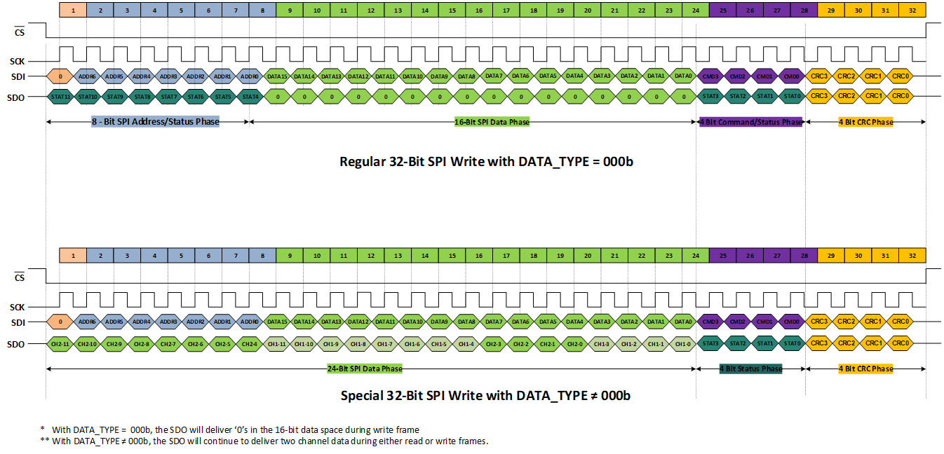
GUID-20210813-SS0I-NZBZ-LVRM-6SMDQ9FSSKRB-low.png Figure 7-15 32-BIT WRITE FRAME