SBASAF4 September 2021 TMAG5170
PRODUCTION DATA
- 1 Features
- 2 Applications
- 3 Description
- 4 Revision History
- 5 Pin Configuration and Functions
- 6 Specifications
-
7 Detailed Description
- 7.1 Overview
- 7.2 Functional Block Diagram
- 7.3
Feature Description
- 7.3.1 Magnetic Flux Direction
- 7.3.2 Sensor Location
- 7.3.3 Magnetic Range Selection
- 7.3.4 Update Rate Settings
- 7.3.5 ALERT Function
- 7.3.6 Threshold Count
- 7.3.7
Diagnostics
- 7.3.7.1 Memory CRC Check
- 7.3.7.2 ALERT Integrity Check
- 7.3.7.3 VCC Check
- 7.3.7.4 Internal LDO Under Voltage Check
- 7.3.7.5 Digital Core Power-on Reset Check
- 7.3.7.6 SDO Output Check
- 7.3.7.7 Communication CRC Check
- 7.3.7.8 Oscillator Integrity Check
- 7.3.7.9 Magnetic Field Threshold Check
- 7.3.7.10 Temperature Alert Check
- 7.3.7.11 Analog Front-End (AFE) Check
- 7.3.7.12 Hall Resistance and Switch Matrix Check
- 7.3.7.13 Hall Offset Check
- 7.3.7.14 ADC Check
- 7.4 Device Functional Modes
- 7.5 Programming
- 7.6 Register Map
- 8 Application and Implementation
- 9 Power Supply Recommendations
- 10Layout
- 11Device and Documentation Support
- 12Mechanical, Packaging, and Orderable Information
Package Options
Mechanical Data (Package|Pins)
- DGK|8
Thermal pad, mechanical data (Package|Pins)
Orderable Information
7.4.1 Operating Modes
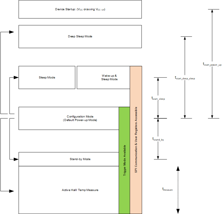
The TMAG5170 supports multiple operating modes for wide array of applications as explained in Figure 7-4. The device starts powering up after the VCC supply crosses the minimum threshold as specified in the Section 6.3 table. Any particular operating mode can be selected by setting the corresponding OPERATING_MODE register bits.
 Figure 7-4 TMAG5170
Power-Up Sequence
Figure 7-4 TMAG5170
Power-Up SequenceTable 7-3 shows different power saving modes of the TMAG5170.
Table 7-3 Comparing Operating
Modes
| OPERATING MODE | DEVICE FUNCTION | INITIALIZATION TIME TO START CONVERSION(1) | DATA CONVERSION |
|---|---|---|---|
| Active Conversion | Continuously measuring X, Y, Z axis, or temperature data | 10 µs | Supports continuous and trigger mode conversion |
| Standby Mode | Device is ready to accept SPI commands and start active conversion | 35 µs | Supports trigger mode conversion |
| Configuration Mode | SPI and user configuration registers active | tstand_by + 35 µs | Supports trigger mode conversion |
| Wake-up & Sleep Mode | Wakes up at a certain interval to measure the X, Y, Z axis, or temperature data | tstart_sleep + tstand_by + 35 µs | 1, 5, 10, 15, 20, 30, 100, 500, and 1000-ms intervals supported(1). |
| Sleep Mode | Device retains key configuration settings, and last measurement data | tstart_sleep + tstand_by + 35 µs | The microcontroller can use sleep mode to implement other power saving intervals not supported by wake-up and sleep mode. |
| Deep-sleep Mode | Device does not retain key configuration settings, and last measurement data | tstart_deep_sleep + tstand_by + 35 µs | No conversion start is supported during deep-sleep mode |
(1) The timing numbers are typical parameters. Their value may vary
depending on the internal oscillator frequency.