SBASAF4 September   2021 TMAG5170

PRODUCTION DATA  

  1. Features
  2. Applications
  3. Description
  4. Revision History
  5. Pin Configuration and Functions
  6. Specifications
    1. 6.1 Absolute Maximum Ratings
    2. 6.2 ESD Ratings
    3. 6.3 Recommended Operating Conditions
    4. 6.4 Thermal Information
    5. 6.5 Electrical Characteristics
    6. 6.6 Magnetic Characteristics
    7. 6.7 Power up Timing
    8. 6.8 SPI Interface Timing
    9. 6.9 Typical Characteristics
  7. Detailed Description
    1. 7.1 Overview
    2. 7.2 Functional Block Diagram
    3. 7.3 Feature Description
      1. 7.3.1 Magnetic Flux Direction
      2. 7.3.2 Sensor Location
      3. 7.3.3 Magnetic Range Selection
      4. 7.3.4 Update Rate Settings
      5. 7.3.5 ALERT Function
        1. 7.3.5.1 Interrupt and Trigger Mode
        2. 7.3.5.2 Magnetic Switch Mode
      6. 7.3.6 Threshold Count
      7. 7.3.7 Diagnostics
        1. 7.3.7.1  Memory CRC Check
        2. 7.3.7.2  ALERT Integrity Check
        3. 7.3.7.3  VCC Check
        4. 7.3.7.4  Internal LDO Under Voltage Check
        5. 7.3.7.5  Digital Core Power-on Reset Check
        6. 7.3.7.6  SDO Output Check
        7. 7.3.7.7  Communication CRC Check
        8. 7.3.7.8  Oscillator Integrity Check
        9. 7.3.7.9  Magnetic Field Threshold Check
        10. 7.3.7.10 Temperature Alert Check
        11. 7.3.7.11 Analog Front-End (AFE) Check
        12. 7.3.7.12 Hall Resistance and Switch Matrix Check
        13. 7.3.7.13 Hall Offset Check
        14. 7.3.7.14 ADC Check
    4. 7.4 Device Functional Modes
      1. 7.4.1 Operating Modes
        1. 7.4.1.1 Active Mode
        2. 7.4.1.2 Standby Mode
        3. 7.4.1.3 Configuration Mode (DEFAULT)
        4. 7.4.1.4 Sleep Mode
        5. 7.4.1.5 Wake-Up and Sleep Mode
        6. 7.4.1.6 Deep-Sleep Mode
    5. 7.5 Programming
      1. 7.5.1 Data Definition
        1. 7.5.1.1 Magnetic Sensor Data
        2. 7.5.1.2 Temperature Sensor Data
        3. 7.5.1.3 Magnetic Sensor Offset Correction
        4. 7.5.1.4 Angle and Magnitude Data Definition
      2. 7.5.2 SPI Interface
        1. 7.5.2.1 SCK
        2. 7.5.2.2 CS
        3. 7.5.2.3 SDI
        4. 7.5.2.4 SDO
          1. 7.5.2.4.1 Regular 32-Bit SDO Read
          2. 7.5.2.4.2 Special 32-Bit SDO Read
        5. 7.5.2.5 SPI CRC
        6. 7.5.2.6 SPI Frame
          1. 7.5.2.6.1 32-Bit Read Frame
          2. 7.5.2.6.2 32-Bit Write Frame
    6. 7.6 Register Map
      1. 7.6.1 TMAG5170 Registers
  8. Application and Implementation
    1. 8.1 Application Information
      1. 8.1.1 Selecting the Sensitivity Option
      2. 8.1.2 Temperature Compensation for Magnets
      3. 8.1.3 Sensor Conversion
        1. 8.1.3.1 Continuous Conversion
        2. 8.1.3.2 Trigger Conversion
        3. 8.1.3.3 Pseudo-Simultaneous Sampling
      4. 8.1.4 Error Calculation During Linear Measurement
      5. 8.1.5 Error Calculation During Angular Measurement
    2. 8.2 Typical Application
      1. 8.2.1 Design Requirements
        1. 8.2.1.1 Gain Adjustment for Angle Measurement
      2. 8.2.2 Detailed Design Procedure
      3. 8.2.3 Application Curves
    3. 8.3 Do's and Don'ts
  9. Power Supply Recommendations
  10. 10Layout
    1. 10.1 Layout Guidelines
    2. 10.2 Layout Example
  11. 11Device and Documentation Support
    1. 11.1 Receiving Notification of Documentation Updates
    2. 11.2 Support Resources
    3. 11.3 Trademarks
    4. 11.4 Electrostatic Discharge Caution
    5. 11.5 Glossary
  12. 12Mechanical, Packaging, and Orderable Information

Package Options

Mechanical Data (Package|Pins)
Thermal pad, mechanical data (Package|Pins)
Orderable Information

SPI CRC

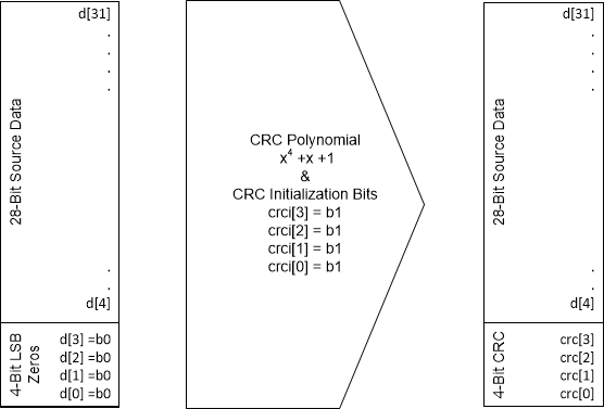
The TMAG5170 performs mandatory CRC for SPI communication. The Data integrity is maintained in both directions by a 4-bit CRC covering the content of the incoming and outgoing 32-bit messages. The four LSB bits of each 32-bit SPI frame are dedicated for the CRC. The CRC code is generated by the polynomial x4 + x + 1. Initialize the CRC bits with b1111.

During the SDI write frame, the TMAG5170 reads for the CRC data before executing a write instruction. The write instruction from the controller is ignored if there is any CRC error present in the frame. During the SDI regular read frame, the TMAG5170 starts to deliver the requested data through SDO line in the same frame and notifies the controller of any error occurrence through the ERROR_STAT bit. If the device detects a CRC error in the SDI line, the device will invert the last bit of the SDO CRC in the same frame to promptly signal to a controller that the SPI communication is compromised. A controller can also determine the presence of a CRC error in the SDI frame by checking the Status11 bit in the next regular read frame.
Note: The TMAG5170 default mode at power up is CRC-enabled. With CRC enabled, the device will ignore all the SDI commands if proper CRC codes are not received. To disable the CRC at the SDI line, send the SPI SDI command x0F000407.
GUID-20200907-CA0I-RDK2-ZQFH-KSPBLPW4PZHM-low.gif Figure 7-13 4-Bit CRC Calculation

Use the following XOR function equations to calculate the 4-bit CRC. Figure 7-13 describes the notations of these equations.

Equation 10. c r c [ 0 ]   =   d [ 30 ]   ^   d [ 26 ]   ^   d [ 25 ]   ^   d [ 24 ]   ^   d [ 23 ]   ^   d [ 21 ]   ^   d [ 19 ]   ^   d [ 18 ]   ^   d [ 15 ]   ^   d [ 11 ]   ^   d [ 10 ]   ^   d [ 9 ]   ^   d [ 8 ]   ^   d [ 6 ]   ^   d [ 4 ]   ^   d [ 3 ]   ^   d [ 0 ]   ^   c r c i [ 2 ]
Equation 11. c r c [ 1 ]   =   d [ 31 ]   ^   d [ 30 ]   ^   d [ 27 ]   ^   d [ 23 ]   ^   d [ 22 ]   ^   d [ 21 ]   ^   d [ 20 ]   ^   d [ 18 ]   ^   d [ 16 ]   ^   d [ 15 ]   ^   d [ 12 ]   ^   d [ 8 ]   ^   d [ 7 ]   ^   d [ 6 ]   ^   d [ 5 ]   ^   d [ 3 ]   ^   d [ 1 ]   ^   d [ 0 ]   ^   c r c i [ 2 ]   ^   c r c i [ 3 ]
Equation 12. c r c [ 2 ]   =   d [ 31 ]   ^   d [ 28 ]   ^   d [ 24 ]   ^   d [ 23 ]   ^   d [ 22 ]   ^   d [ 21 ]   ^   d [ 19 ]   ^   d [ 17 ]   ^   d [ 16 ]   ^   d [ 13 ]   ^   d [ 9 ]   ^   d [ 8 ]   ^   d [ 7 ]   ^   d [ 6 ]   ^   d [ 4 ]   ^   d [ 2 ]   ^   d [ 1 ]   ^   c r c i [ 0 ]   ^   c r c i [ 3 ]
Equation 13. c r c [ 3 ]   =   d [ 29 ]   ^   d [ 25 ]   ^   d [ 24 ]   ^   d [ 23 ]   ^   d [ 22 ]   ^   d [ 20 ]   ^   d [ 18 ]   ^   d [ 17 ]   ^   d [ 14 ]   ^   d [ 10 ]   ^   d [ 9 ]   ^   d [ 8 ]   ^   d [ 7 ]   ^   d [ 5 ]   ^   d [ 3 ]   ^   d [ 2 ]   ^   c r c i [ 1 ]

The following shows example codes for calculating the 4-bit CRC.

function logic [3:0] calculate_crc4;
   input logic [27:0] frame;

   logic [31:0]       padded_frame;
   logic [3:0] 	      frame_crc;
   logic 	      inv;
   integer 	      i;

   padded_frame = {frame, 4'b0000};
   
   begin
      frame_crc = 4'hf; // initial value
      for (i=31; i >= 0; i=i-1) begin
	 inv = padded_frame[i] ^ frame_crc[3];
	 frame_crc[3] = frame_crc[2];
	 frame_crc[2] = frame_crc[1];
	 frame_crc[1] = frame_crc[0] ^ inv;
	 frame_crc[0] = inv;
      end
      return frame_crc;
   end
endfunction