SBOSA43 June 2021 TMCS1100-Q1
PRODUCTION DATA
- 1 Features
- 2 Applications
- 3 Description
- 4 Revision History
- 5 Device Comparison
- 6 Pin Configuration and Functions
- 7 Specifications
- 8 Parameter Measurement Information
- 9 Detailed Description
- 10Application and Implementation
- 11Power Supply Recommendations
- 12Layout
- 13Device and Documentation Support
- 14Mechanical, Packaging, and Orderable Information
Package Options
Refer to the PDF data sheet for device specific package drawings
Mechanical Data (Package|Pins)
- D|8
Thermal pad, mechanical data (Package|Pins)
Orderable Information
12.1 Layout Guidelines
The TMCS1100-Q1 is specified for a continuous current handling capability on the TMCS1100EVM, which uses 3-oz copper pour planes. This current capability is fundamentally limited by the maximum device junction temperature and the thermal environment, primarily the PCB layout and design. To maximize current-handling capability and thermal stability of the device, take care with PCB layout and construction to optimize the thermal capability. Efforts to improve the thermal performance beyond the design and construction of the TMCS1100EVM can result in increased continuous-current capability due to higher heat transfer to the ambient environment. Keys to improving thermal performance of the PCB include:
- Use large copper planes for both input current path and isolated power planes and signals.
- Use heavier copper PCB construction.
- Place thermal via farms around the isolated current input.
- Provide airflow across the surface of the PCB.
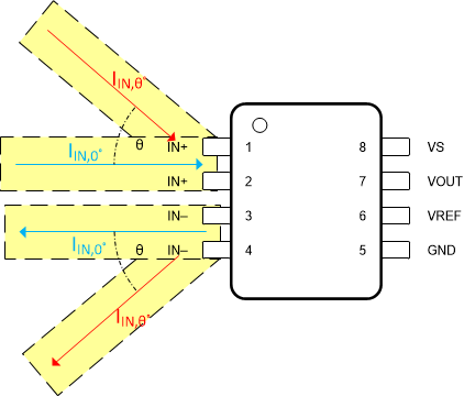
The TMCS1100-Q1 senses external magnetic fields, so make sure to minimize adjacent high-current traces in close proximity to the device. The input current trace can contribute additional magnetic field to the sensor if the input current traces are routed parallel to the vertical axis of the package. Figure 12-1 illustrates the most optimal input current routing into the TMCS1100-Q1. As the angle that the current approaches the device deviates from 0° to the horizontal axis, the current trace contributes some additional magnetic field to the sensor, increasing the effective sensitivity of the device. If current must be routed parallel to the package vertical axis, move the routing away from the package to minimize the impact to the sensitivity of the device. Terminate the input current path directly underneath the package lead footprint, and use a merged copper input trace for both the IN+ and IN– inputs.
 Figure 12-1 Magnetic Field Generated by Input Current Trace
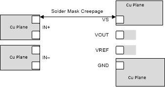
In addition to thermal and magnetic optimization, make sure to consider the PCB design required creepage and clearance for system-level isolation requirements. Maintain required creepage between solder stencils, as shown in Figure 12-2, if possible. If not possible to maintain required PCB creepage between the two isolated sides at board level, add additional slots or grooves to the board. If more creepage and clearance is required for system isolation levels than is provided by the package, the entire device and solder mask can be encapsulated with an overmold compound to meet system-level requirements.
 Figure 12-2 Layout for System Creepage Requirements