SBOS825D September   2019  – July 2021 TMCS1101

PRODUCTION DATA  

  1. Features
  2. Applications
  3. Description
  4. Revision History
  5. Device Comparison
  6. Pin Configuration and Functions
  7. Specifications
    1. 7.1  Absolute Maximum Ratings
    2. 7.2  ESD Ratings
    3. 7.3  Recommended Operating Conditions
    4. 7.4  Thermal Information
    5. 7.5  Power Ratings
    6. 7.6  Insulation Specifications
    7. 7.7  Safety-Related Certifications
    8. 7.8  Safety Limiting Values
    9. 7.9  Electrical Characteristics
    10. 7.10 Typical Characteristics
      1. 7.10.1 Insulation Characteristics Curves
  8. Parameter Measurement Information
    1. 8.1 Accuracy Parameters
      1. 8.1.1 Sensitivity Error
      2. 8.1.2 Offset Error and Offset Error Drift
      3. 8.1.3 Nonlinearity Error
      4. 8.1.4 Power Supply Rejection Ratio
      5. 8.1.5 Common-Mode Rejection Ratio
      6. 8.1.6 External Magnetic Field Errors
    2. 8.2 Transient Response Parameters
      1. 8.2.1 Slew Rate
      2. 8.2.2 Propagation Delay and Response Time
      3. 8.2.3 Current Overload Parameters
      4. 8.2.4 CMTI, Common-Mode Transient Immunity
    3. 8.3 Safe Operating Area
      1. 8.3.1 Continuous DC or Sinusoidal AC Current
      2. 8.3.2 Repetitive Pulsed Current SOA
      3. 8.3.3 Single Event Current Capability
  9. Detailed Description
    1. 9.1 Overview
    2. 9.2 Functional Block Diagram
    3. 9.3 Feature Description
      1. 9.3.1 Current Input
      2. 9.3.2 Input Isolation
      3. 9.3.3 High-Precision Signal Chain
        1. 9.3.3.1 Temperature Stability
        2. 9.3.3.2 Lifetime and Environmental Stability
        3. 9.3.3.3 Frequency Response
        4. 9.3.3.4 Transient Response
      4. 9.3.4 Internal Reference Voltage
      5. 9.3.5 Current-Sensing Measurable Ranges
    4. 9.4 Device Functional Modes
      1. 9.4.1 Power-Down Behavior
  10. 10Application and Implementation
    1. 10.1 Application Information
      1. 10.1.1 Total Error Calculation Examples
        1. 10.1.1.1 Room Temperature Error Calculations
        2. 10.1.1.2 Full Temperature Range Error Calculations
    2. 10.2 Typical Application
      1. 10.2.1 Design Requirements
      2. 10.2.2 Detailed Design Procedure
  11. 11Power Supply Recommendations
  12. 12Layout
    1. 12.1 Layout Guidelines
    2. 12.2 Layout Example
  13. 13Device and Documentation Support
    1. 13.1 Device Support
      1. 13.1.1 Development Support
    2. 13.2 Documentation Support
      1. 13.2.1 Related Documentation
    3. 13.3 Receiving Notification of Documentation Updates
    4. 13.4 Support Resources
    5. 13.5 Trademarks
    6. 13.6 Electrostatic Discharge Caution
    7. 13.7 Glossary
  14. 14Mechanical, Packaging, and Orderable Information

Package Options

Refer to the PDF data sheet for device specific package drawings

Mechanical Data (Package|Pins)
  • D|8
Thermal pad, mechanical data (Package|Pins)
Orderable Information

Temperature Stability

The TMCS1101 includes a proprietary temperature compensation technique which results in significantly improved parametric drift across the full temperature range. This compensation technique accounts for changes in ambient temperature, self-heating, and package stress. A zero-drift signal chain architecture and Hall sensor temperature stabilization methods enable stable sensitivity and minimize offset errors across temperature, and drastically improves system-level performance across the required operating conditions.

Figure 9-2 and Figure 9-3 show the offset error across the full device ambient temperature range. Figure 9-4 and Figure 9-5 show the typical sensitivity. There are no other external components introducing errors sources; therefore, the high intrinsic accuracy and stability over temperature directly translates to system-level performance. As a result of this high precision, even a system with no calibration can reach < 1.5% of total error current-sensing capability.
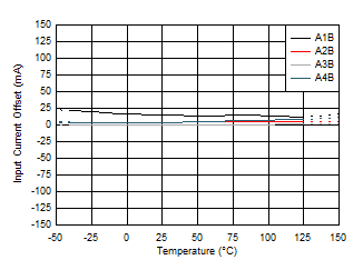
GUID-59B97934-8797-4B58-9BCF-E7625CB10B5D-low.gifFigure 9-2 Offset Error Drift Across Temperature (B Variants)
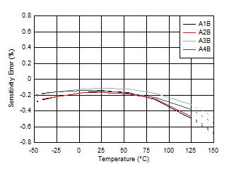
GUID-CA6CBE21-9C2D-4024-9D92-5CA4032CA007-low.gifFigure 9-4 Sensitivity Drift Across Temperature (B Variants)
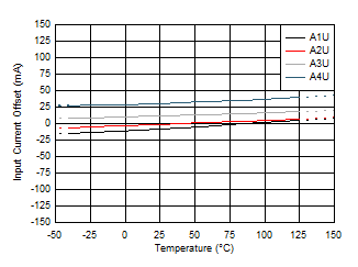
GUID-2B2D2D13-7E42-4A22-9026-AB0FAA5BA351-low.gifFigure 9-3 Offset Error Drift Across Temperature (U Variants)
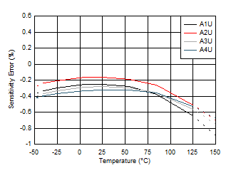
GUID-452ABA93-BA50-4B88-8C8F-F4D0531874D1-low.gifFigure 9-5 Sensitivity Drift Across Temperature (U Variants)