SBOS825D September   2019  – July 2021 TMCS1101

PRODUCTION DATA  

  1. Features
  2. Applications
  3. Description
  4. Revision History
  5. Device Comparison
  6. Pin Configuration and Functions
  7. Specifications
    1. 7.1  Absolute Maximum Ratings
    2. 7.2  ESD Ratings
    3. 7.3  Recommended Operating Conditions
    4. 7.4  Thermal Information
    5. 7.5  Power Ratings
    6. 7.6  Insulation Specifications
    7. 7.7  Safety-Related Certifications
    8. 7.8  Safety Limiting Values
    9. 7.9  Electrical Characteristics
    10. 7.10 Typical Characteristics
      1. 7.10.1 Insulation Characteristics Curves
  8. Parameter Measurement Information
    1. 8.1 Accuracy Parameters
      1. 8.1.1 Sensitivity Error
      2. 8.1.2 Offset Error and Offset Error Drift
      3. 8.1.3 Nonlinearity Error
      4. 8.1.4 Power Supply Rejection Ratio
      5. 8.1.5 Common-Mode Rejection Ratio
      6. 8.1.6 External Magnetic Field Errors
    2. 8.2 Transient Response Parameters
      1. 8.2.1 Slew Rate
      2. 8.2.2 Propagation Delay and Response Time
      3. 8.2.3 Current Overload Parameters
      4. 8.2.4 CMTI, Common-Mode Transient Immunity
    3. 8.3 Safe Operating Area
      1. 8.3.1 Continuous DC or Sinusoidal AC Current
      2. 8.3.2 Repetitive Pulsed Current SOA
      3. 8.3.3 Single Event Current Capability
  9. Detailed Description
    1. 9.1 Overview
    2. 9.2 Functional Block Diagram
    3. 9.3 Feature Description
      1. 9.3.1 Current Input
      2. 9.3.2 Input Isolation
      3. 9.3.3 High-Precision Signal Chain
        1. 9.3.3.1 Temperature Stability
        2. 9.3.3.2 Lifetime and Environmental Stability
        3. 9.3.3.3 Frequency Response
        4. 9.3.3.4 Transient Response
      4. 9.3.4 Internal Reference Voltage
      5. 9.3.5 Current-Sensing Measurable Ranges
    4. 9.4 Device Functional Modes
      1. 9.4.1 Power-Down Behavior
  10. 10Application and Implementation
    1. 10.1 Application Information
      1. 10.1.1 Total Error Calculation Examples
        1. 10.1.1.1 Room Temperature Error Calculations
        2. 10.1.1.2 Full Temperature Range Error Calculations
    2. 10.2 Typical Application
      1. 10.2.1 Design Requirements
      2. 10.2.2 Detailed Design Procedure
  11. 11Power Supply Recommendations
  12. 12Layout
    1. 12.1 Layout Guidelines
    2. 12.2 Layout Example
  13. 13Device and Documentation Support
    1. 13.1 Device Support
      1. 13.1.1 Development Support
    2. 13.2 Documentation Support
      1. 13.2.1 Related Documentation
    3. 13.3 Receiving Notification of Documentation Updates
    4. 13.4 Support Resources
    5. 13.5 Trademarks
    6. 13.6 Electrostatic Discharge Caution
    7. 13.7 Glossary
  14. 14Mechanical, Packaging, and Orderable Information

Package Options

Refer to the PDF data sheet for device specific package drawings

Mechanical Data (Package|Pins)
  • D|8
Thermal pad, mechanical data (Package|Pins)
Orderable Information

Mechanical, Packaging, and Orderable Information

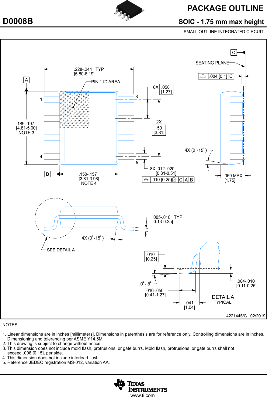
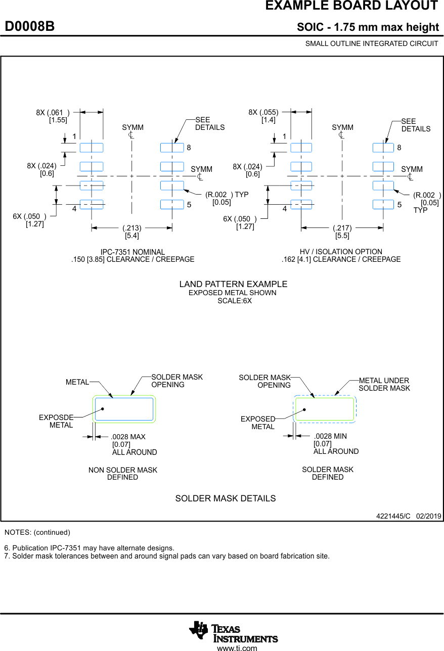
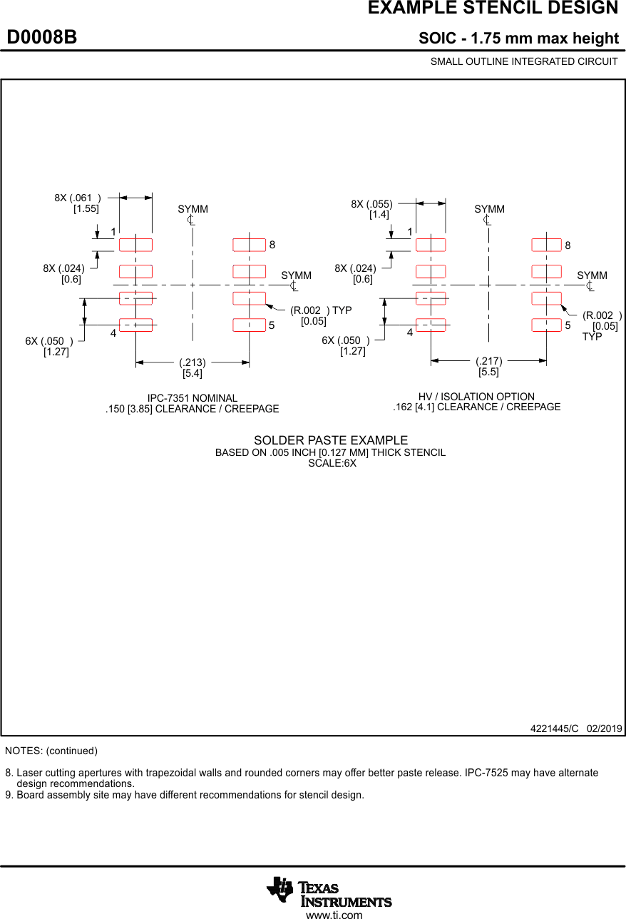
The following pages include mechanical, packaging, and orderable information. This information is the most current data available for the designated devices. This data is subject to change without notice and revision of this document. For browser-based versions of this data sheet, refer to the left-hand navigation.
GUID-E999F6E3-0203-444A-A0E8-DF5FE5DA0985-low.gif

GUID-7CC0E310-E291-4174-9F09-7470ACDFC0C3-low.gif

GUID-047EA902-DA28-4F0A-8377-CA8E269FE165-low.gif