SBOS397I August   2007  – June 2024 TMP102

PRODUCTION DATA  

  1.   1
  2. Features
  3. Applications
  4. Description
  5. Pin Configuration and Functions
  6. Specifications
    1. 5.1 Absolute Maximum Ratings
    2. 5.2 ESD Ratings
    3. 5.3 Recommended Operating Conditions
    4. 5.4 Thermal Information
    5. 5.5 Electrical Characteristics
    6. 5.6 Timing Requirements
    7. 5.7 Typical Characteristics
  7. Detailed Description
    1. 6.1 Overview
    2. 6.2 Functional Block Diagram
    3. 6.3 Feature Description
      1. 6.3.1  Digital Temperature Output
      2. 6.3.2  Serial Interface
      3. 6.3.3  Bus Overview
      4. 6.3.4  Serial Bus Address
      5. 6.3.5  Writing and Reading Operation
      6. 6.3.6  Target Mode Operations
        1. 6.3.6.1 Target Receiver Mode
        2. 6.3.6.2 Target Transmitter Mode
      7. 6.3.7  SMBus Alert Function
      8. 6.3.8  General Call
      9. 6.3.9  High-Speed (HS) Mode
      10. 6.3.10 Timeout Function
      11. 6.3.11 Timing Diagrams
    4. 6.4 Device Functional Modes
      1. 6.4.1 Continuous-Conversion Mode
      2. 6.4.2 Extended Mode (EM)
      3. 6.4.3 Shutdown Mode (SD)
      4. 6.4.4 One-Shot/Conversion Ready (OS)
      5. 6.4.5 Thermostat Mode (TM)
        1. 6.4.5.1 Comparator Mode (TM = 0)
        2. 6.4.5.2 Interrupt Mode (TM = 1)
    5. 6.5 Programming
      1. 6.5.1 Pointer Register
      2. 6.5.2 Temperature Register
      3. 6.5.3 Configuration Register
        1. 6.5.3.1 Shutdown Mode (SD)
        2. 6.5.3.2 Thermostat Mode (TM)
        3. 6.5.3.3 Polarity (POL)
        4. 6.5.3.4 Fault Queue (F1/F0)
        5. 6.5.3.5 Converter Resolution (R1/R0)
        6. 6.5.3.6 One-Shot (OS)
        7. 6.5.3.7 EM Bit
        8. 6.5.3.8 Alert (AL Bit)
        9. 6.5.3.9 Conversion Rate (CR)
      4. 6.5.4 High- and Low-Limit Registers
  8. Application and Implementation
    1. 7.1 Application Information
    2. 7.2 Typical Application
      1. 7.2.1 Design Requirements
      2. 7.2.2 Detailed Design Procedure
      3. 7.2.3 Application Curve
    3. 7.3 Power Supply Recommendations
    4. 7.4 Layout
      1. 7.4.1 Layout Guidelines
      2. 7.4.2 Layout Example
  9. Device and Documentation Support
    1. 8.1 Documentation Support
      1. 8.1.1 Related Documentation
    2. 8.2 Receiving Notification of Documentation Updates
    3. 8.3 Support Resources
    4. 8.4 Trademarks
    5. 8.5 Electrostatic Discharge Caution
    6. 8.6 Glossary
  10. Revision History
  11. 10Mechanical, Packaging, and Orderable Information

Package Options

Mechanical Data (Package|Pins)
Thermal pad, mechanical data (Package|Pins)
Orderable Information

Pointer Register

Figure 6-6 illustrates the internal register structure of the TMP102 device. The 8-bit Pointer Register of the device is used to address a given data register. The Pointer Register uses the two least-significant bytes (LSBs) (see Table 6-15 and Table 6-16) to identify which of the data registers must respond to a read or write command. Table 6-6 identifies the bits of the Pointer Register byte. During a write command, P2 through P7 must always be '0'. Table 6-7 describes the pointer address of the registers available in the TMP102 device. The power-up reset value of P1 and P0 is 00. By default, the TMP102 device reads the temperature on power up.
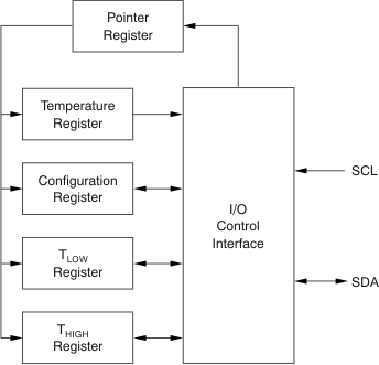
TMP102 Internal Register StructureFigure 6-6 Internal Register Structure
Table 6-6 Pointer Register Byte
P7P6P5P4P3P2P1P0
000000Register Bits
Table 6-7 Pointer Addresses
P1 P0 REGISTER
0 0 Temperature Register (Read Only)
0 1 Configuration Register (Read/Write)
1 0 TLOW Register (Read/Write)
1 1 THIGH Register (Read/Write)