SBOS564B November 2011 – December 2018 TMP104
PRODUCTION DATA.
- 1Features
- 2Applications
- 3Description
- 4Revision History
- 5Pin Configuration and Functions
- 6Specifications
- 7Detailed Description
- 8Device and Documentation Support
- 9Mechanical, Packaging, and Orderable Information
Package Options
Refer to the PDF data sheet for device specific package drawings
Mechanical Data (Package|Pins)
- YFF|4
Thermal pad, mechanical data (Package|Pins)
Orderable Information
7.3.7 Individual Read and Write
The host can initiate an individual read/write command to a particular TMP104 in the daisy-chain by sending the read/write command. The read/write command consists of these parameters:
- P7 = 0
- P6-P3 = the device ID
- P2-P1 = the data register pointer; see Table 4
- P0 = indicates read/write control
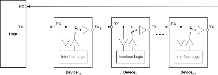
P0 = 0 indicates an individual write command; the host must transfer one more byte of data for the register indicated by bits P2-P1. The TMP104 in the daisy-chain that corresponds to the device ID noted by bits P6-P3 then updates the appropriate register. P0 = 1 indicates an individual read command; as shown in Figure 12, the TMP104 in the daisy-chain that corresponds to the device ID pointed by bits P6-P3 then breaks the bus, transmits the data from the register pointed by bits P2-P1, and reconnects the bus.
 Figure 12. TMP104 Daisy-Chain: Bus Status During Individual Read Operation of Second Device