SNIS227C May   2021  – June 2022 TMP126-Q1

PRODUCTION DATA  

  1. Features
  2. Applications
  3. Description
  4. Revision History
  5. Device Comparison
  6. Pin Configuration and Functions
  7. Specifications
    1. 7.1 Absolute Maximum Ratings
    2. 7.2 ESD Ratings
    3. 7.3 Recommended Operating Conditions
    4. 7.4 Thermal Information
    5. 7.5 Electrical Characteristics
    6. 7.6 SPI Interface Timing
    7. 7.7 Typical Characteristics
  8. Detailed Description
    1. 8.1 Overview
    2. 8.2 Functional Block Diagram
    3. 8.3 Feature Descriptions
      1. 8.3.1 Temperature Limits
      2. 8.3.2 Slew Rate Warning
      3. 8.3.3 Cyclic Redundancy Check (CRC)
      4. 8.3.4 NIST Traceability
      5. 8.3.5 Fast Measurement Intervals With No Self-Heating Concerns
    4. 8.4 Device Functional Modes
      1. 8.4.1 Continuous Conversion Mode
      2. 8.4.2 Shutdown Mode
      3. 8.4.3 One-Shot Mode
      4. 8.4.4 Interrupt and Comparator Mode
        1. 8.4.4.1 Interrupt Mode
        2. 8.4.4.2 Comparator Mode
    5. 8.5 Programming
      1. 8.5.1 Temperature Data Format
      2. 8.5.2 Serial Bus Interface
        1. 8.5.2.1 Command Word Structure
          1. 8.5.2.1.1 Don't Care
          2. 8.5.2.1.2 CRC Enable
          3. 8.5.2.1.3 CRC Data Block Length
          4. 8.5.2.1.4 Auto Increment
          5. 8.5.2.1.5 Read/Write
          6. 8.5.2.1.6 Sub-Address
        2. 8.5.2.2 Communication
        3. 8.5.2.3 Write Operations
        4. 8.5.2.4 Read Operations
        5. 8.5.2.5 Cyclic Redundancy Check (CRC)
          1. 8.5.2.5.1 Cyclic Redundancy Check Implementation
    6. 8.6 Register Map
  9. Application and Implementation
    1. 9.1 Application Information
    2. 9.2 Typical Application
      1. 9.2.1 Design Requirements
      2. 9.2.2 Detailed Design Procedure
  10. 10Power Supply Recommendations
  11. 11Layout
    1. 11.1 Layout Guidelines
    2. 11.2 Layout Example
  12. 12Device and Documentation Support
    1. 12.1 Documentation Support
      1. 12.1.1 Related Documentation
    2. 12.2 Receiving Notification of Documentation Updates
    3. 12.3 Support Resources
    4. 12.4 Trademarks
    5. 12.5 Electrostatic Discharge Caution
    6. 12.6 Glossary
  13. 13Mechanical, Packaging, and Orderable Information

Package Options

Mechanical Data (Package|Pins)
Thermal pad, mechanical data (Package|Pins)
Orderable Information

Description

The TMP126-Q1 is a 0.25°C accuracy digital temperature that supports an ambient temperature range of –55°C to 175°C. The TMP126-Q1 features a 14-bit signed temperature resolution (0.03125°C per LSB) while operating over a supply range of 1.62 V to 5.5 V. With a fast conversion rate, low supply current, and a simple 3-wire SPI compatible interface, the TMP126-Q1 is designed for a wide range of applications.

The TMP126-Q1 includes additional advanced features for increased reliability in harsh environments such as optional CRC checksum for data integrity, programmable alert limits, a temperature slew rate warning, and an enhanced operational temperature range. The device utilizes a NIST traceable factory calibration for guaranteed accuracy and comes in a small SOT package for close placement to heat sources along with fast response times.

Device Information
PART NUMBERPACKAGE(1)BODY SIZE (NOM)
TMP126-Q1SOT-SC70 (6)2.00 mm × 1.25 mm
SOT-23 (6)2.90 mm × 1.60 mm
For all available packages, see the orderable addendum at the end of the data sheet.
Simplified Application
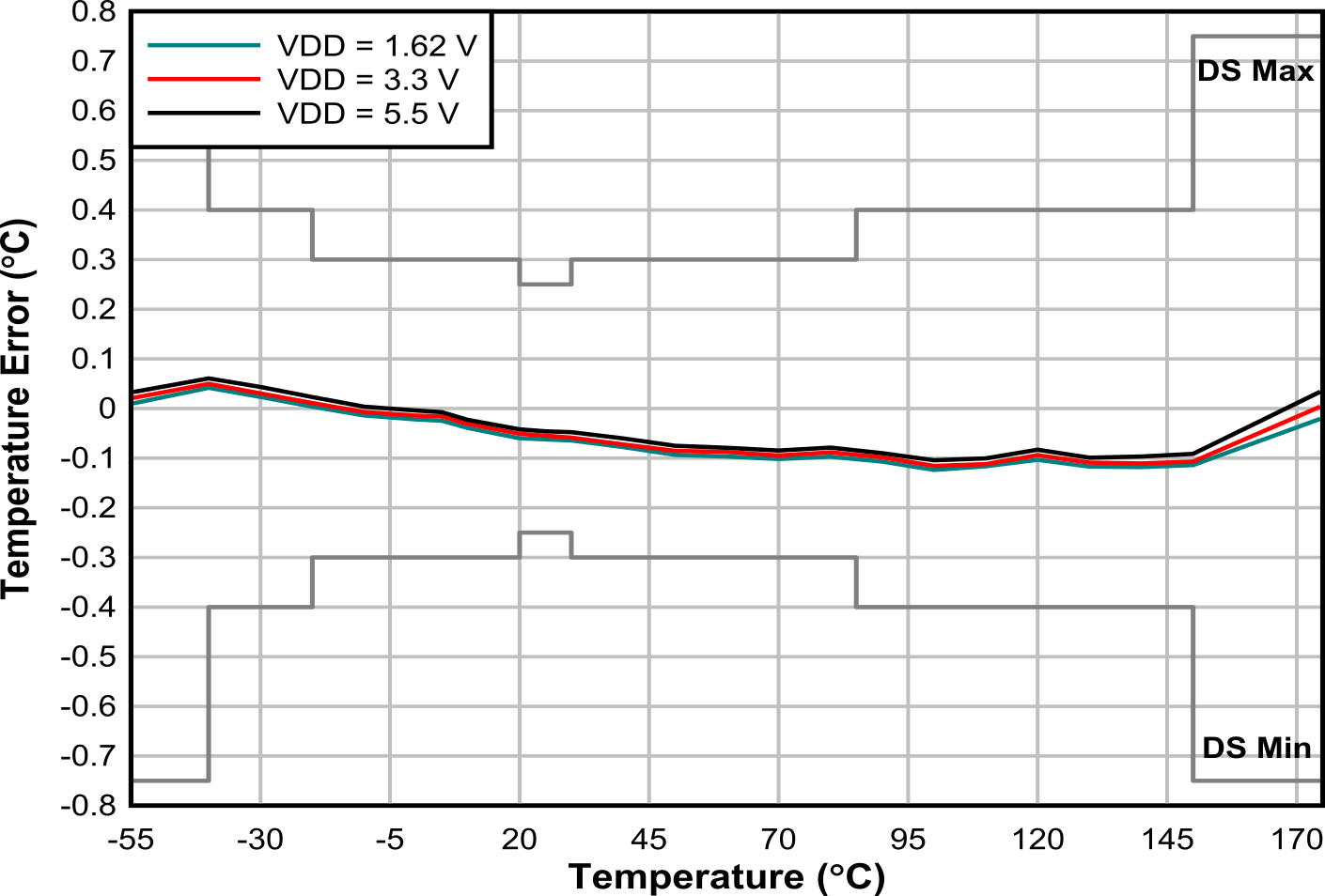
GUID-FB6A91BC-2A55-4494-9E92-A3FC2F7D4E13-low.pngAverage Temperature Accuracy (DBV)