SNIS227C May 2021 – June 2022 TMP126-Q1
PRODUCTION DATA
- 1 Features
- 2 Applications
- 3 Description
- 4 Revision History
- 5 Device Comparison
- 6 Pin Configuration and Functions
- 7 Specifications
-
8 Detailed Description
- 8.1 Overview
- 8.2 Functional Block Diagram
- 8.3 Feature Descriptions
- 8.4 Device Functional Modes
- 8.5 Programming
- 8.6 Register Map
- 9 Application and Implementation
- 10Power Supply Recommendations
- 11Layout
- 12Device and Documentation Support
- 13Mechanical, Packaging, and Orderable Information
Package Options
Mechanical Data (Package|Pins)
Thermal pad, mechanical data (Package|Pins)
Orderable Information
8.4.3 One-Shot Mode
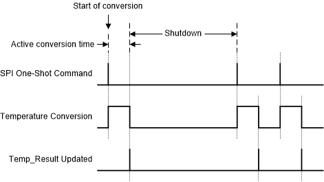
When One_Shot bit is set to 1 in the Configuration register the TMP126-Q1 will immediately start a new temperature conversion, referred to as a one-shot conversion, and discard any partial conversion results. After the device completes a one-shot conversion, the device will enter the low power shutdown mode. The Mode bit will be set to 1 and the One_Shot bit will be set to 0 automatically. Figure 8-5 shows a current consumption timing diagram for this mode. At the end of a one-shot conversion, the Data_Ready_Flag in the Alert_Status register is set and can be used to determine when the conversion completes.
 Figure 8-5 One-Shot Timing Diagram
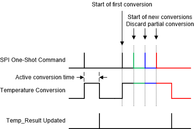
If the One_Shot bit is continuously written to faster than the active conversion time of the TMP126, the device will continue to restart the temperature conversion with each new write. It is recommended to avoid this behavior as the temperature result does not update until a conversion finishes. If continuous one-shots are being triggered by the system Figure 8-6 depicts how the device would continually partially finish new conversions and not update the Temp_Result register.
 Figure 8-6 One-Shot Continuous Trigger Timing Diagram