SNIS209C July   2021  – June 2022 TMP126

PRODUCTION DATA  

  1. Features
  2. Applications
  3. Description
  4. Revision History
  5. Device Comparison
  6. Pin Configuration and Functions
  7. Specifications
    1. 7.1 Absolute Maximum Ratings
    2. 7.2 ESD Ratings
    3. 7.3 Recommended Operating Conditions
    4. 7.4 Thermal Information
    5. 7.5 Electrical Characteristics
    6. 7.6 SPI Interface Timing
    7. 7.7 Timing Diagram
    8. 7.8 Typical Characteristics
  8. Detailed Description
    1. 8.1 Overview
    2. 8.2 Functional Block Diagram
    3. 8.3 Feature Descriptions
      1. 8.3.1 Temperature Limits
      2. 8.3.2 Slew Rate Warning
      3. 8.3.3 Cyclic Redundancy Check (CRC)
      4. 8.3.4 NIST Traceability
      5. 8.3.5 Fast Measurement Intervals With No Self-Heating Concerns
    4. 8.4 Device Functional Modes
      1. 8.4.1 Continuous Conversion Mode
      2. 8.4.2 Shutdown Mode
      3. 8.4.3 One-Shot Mode
      4. 8.4.4 Interrupt and Comparator Mode
        1. 8.4.4.1 Interrupt Mode
        2. 8.4.4.2 Comparator Mode
    5. 8.5 Programming
      1. 8.5.1 Temperature Data Format
      2. 8.5.2 Serial Bus Interface
        1. 8.5.2.1 Command Word Structure
          1. 8.5.2.1.1 Don't Care
          2. 8.5.2.1.2 CRC Enable
          3. 8.5.2.1.3 CRC Data Block Length
          4. 8.5.2.1.4 Auto Increment
          5. 8.5.2.1.5 Read/Write
          6. 8.5.2.1.6 Sub-Address
        2. 8.5.2.2 Communication
        3. 8.5.2.3 Write Operations
        4. 8.5.2.4 Read Operations
        5. 8.5.2.5 Cyclic Redundancy Check (CRC)
          1. 8.5.2.5.1 Cyclic Redundancy Check Implementation
    6. 8.6 Register Map
  9. Application and Implementation
    1. 9.1 Application Information
    2. 9.2 Typical Application
      1. 9.2.1 Design Requirements
      2. 9.2.2 Detailed Design Procedure
      3. 9.2.3 Application Curve
  10. 10Power Supply Recommendations
  11. 11Layout
    1. 11.1 Layout Guidelines
    2. 11.2 Layout Example
  12. 12Device and Documentation Support
    1. 12.1 Documentation Support
      1. 12.1.1 Related Documentation
    2. 12.2 Receiving Notification of Documentation Updates
    3. 12.3 Support Resources
    4. 12.4 Trademarks
    5. 12.5 Electrostatic Discharge Caution
    6. 12.6 Glossary
  13. 13Mechanical, Packaging, and Orderable Information

Package Options

Mechanical Data (Package|Pins)
Thermal pad, mechanical data (Package|Pins)
Orderable Information
Cyclic Redundancy Check Implementation

Table 8-2 defines the CRC calculation rule.

Table 8-2 CRC Rule Table
TemperatureDigital Output
CRC Width16 bits
PolynomialX16 + X12 + X5 + 1 (1021h)
Initial seed valueFFFFh
Input data reflectedNo
Result data reflectedNo
XOR value0000h
ExampleCRC of 0xABCD = 0xD46A

Figure 8-17 shows the CRC Module block diagram. The CRC calculation is done on the command word and the data block. The module consists of a 16-bit shift register and 3 exclusive-OR gates. The register starts with the seed value FFFFh and the module performs an XOR function and shifts its content until the last bit of the register string is used. The final value of the shift register checksum is output onto the SIO line by the TMP126 at the end of the data block for the host to validate the transaction.

GUID-369B5C65-A0FA-43DB-A58D-20F8F62E5529-low.gifFigure 8-17 CRC Module

The following is an example of C code programming example to calculative the communication CRC:
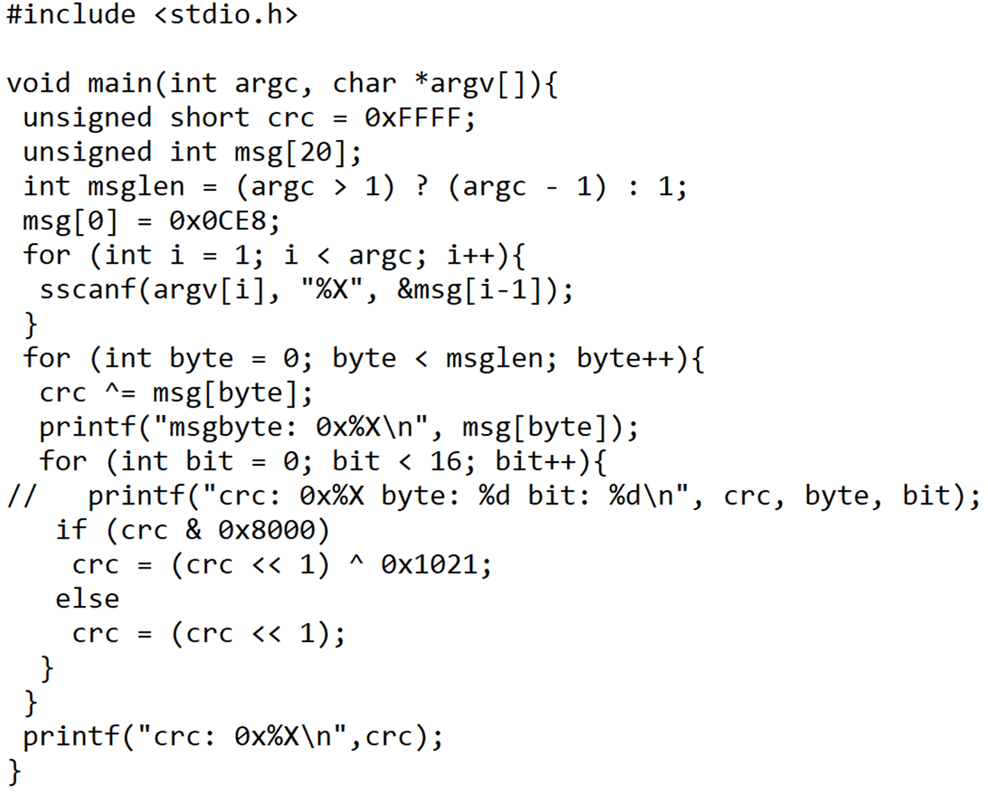
GUID-95C87851-CFFF-4CC3-9494-E201DBE8EF53-low.gif Figure 8-18 CRC Calculation C Code Example.