SBOS760B November 2015 – April 2017 TMP275-Q1
PRODUCTION DATA.
- 1 Features
- 2 Applications
- 3 Description
- 4 Revision History
- 5 Pin Configuration and Functions
- 6 Specifications
- 7 Detailed Description
- 8 Application and Implementation
- 9 Power Supply Recommendations
- 10Layout
- 11Device and Documentation Support
- 12Mechanical, Packaging, and Orderable Information
Package Options
Mechanical Data (Package|Pins)
Thermal pad, mechanical data (Package|Pins)
Orderable Information
1 Features
- AEC-Q100 Qualified with:
- Temperature Grade 1: –40°C to +125°C Ambient Operation Temperature Range
- HBM ESD Classification Level 2
- CDM ESD Classification Level C6
- High Accuracy:
- ±0.75°C (Maximum) from −10°C to +85°C
- ±1.5°C (Maximum) from −40°C to +125°C
- Low Quiescent Current:
- 50 μA (Typical)
- 0.1 μA (Standby)
- Resolution: 9 to 12 Bits, User-Selectable
- Digital Output: SMBus™, Two-Wire, and I2C Interface Compatibility
- 8 I2C, SMBus Addresses
- Wide Supply Range: 2.7 V to 5.5 V
- Small 8-Pin VSSOP and SOIC Packages
- No Specified Power-Up Sequence Required, Two-Wire Bus Pullups Can Be Enabled Before V+
2 Applications
- Climate Controls
- Infotainment Processor Management
- Airflow Sensors
- Battery Control Units
- Engine Control Units
- UREA Sensors
- Water Pumps
- HID Lamps
- Airbag Control Units
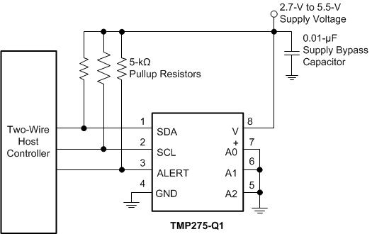
Simplified Schematic

3 Description
The TMP275-Q1 is a ±0.75°C, accurate integrated digital temperature sensor with a 12-bit, analog-to-digital converter (ADC) that can operate on a supply voltage as low as 2.7 V and is pin- and register-compatible with the Texas Instruments' LM75, TMP75, TMP75B, and TMP175 devices. The TMP275-Q1 device is available in 8-pin SOIC and VSSOP packages and requires no external components to sense temperature. The device is capable of reading temperatures with a maximum resolution of 0.0625°C (12 bits) and as low as 0.5°C (9 bits), thus allowing the user to maximize efficiency by programming for higher resolution or faster conversion time. The device is specified over the temperature range of –40°C to +125°C.
The TMP275-Q1 device features SMBus and two-wire interface compatibility and allows up to eight devices on the same bus with the SMBus overtemperature alert function. The factory-calibrated temperature accuracy and the noise-immune digital interface make the TMP275-Q1 the preferred solution for temperature compensation of other sensors and electronic components, without the need for additional system-level calibration or elaborate board layout for distributed temperature sensing.
Device Information(1)
| PART NUMBER | PACKAGE | BODY SIZE (NOM) |
|---|---|---|
| TMP275-Q1 | SOIC (8) | 4.90 mm × 3.91 mm |
| VSSOP (8) | 3.00 mm × 3.00 mm |
- For all available packages, see the package option addendum at the end of the data sheet.
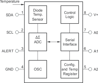
Internal Block Diagram

4 Revision History
Changes from A Revision (January 2016) to B Revision
- Changed temperature (maximum) in title, Features and Description from "±0.5°C" to "±0.75°C"; change temperature range under "High Accuracy" row for ±0.75°C from "–20°C to 100°C" to "–10°C to 85°C"Go
- Changed first test condition temperature range in "Accuracy" row from "–20°C to 100°C" to "–10°C to 85°C"; change MAX value in same row from "±0.5°C" to "±0.75°C"Go
Changes from * Revision (November 2015) to A Revision
- Changed Thermal Information table specificationsGo