SBOS760B November   2015  – April 2017 TMP275-Q1

PRODUCTION DATA.  

  1. Features
  2. Applications
  3. Description
  4. Revision History
  5. Pin Configuration and Functions
  6. Specifications
    1. 6.1 Absolute Maximum Ratings
    2. 6.2 ESD Ratings
    3. 6.3 Recommended Operating Conditions
    4. 6.4 Thermal Information
    5. 6.5 Electrical Characteristics
    6. 6.6 Timing Requirements
    7. 6.7 Typical Characteristics
  7. Detailed Description
    1. 7.1 Overview
    2. 7.2 Functional Block Diagram
    3. 7.3 Feature Description
      1. 7.3.1 Digital Temperature Output
      2. 7.3.2 Serial Interface
      3. 7.3.3 Bus Overview
      4. 7.3.4 Serial Bus Address
        1. 7.3.4.1 Writing and Reading to the TMP275-Q1
        2. 7.3.4.2 Slave Mode Operations
          1. 7.3.4.2.1 Slave Receiver Mode
          2. 7.3.4.2.2 Slave Transmitter Mode
        3. 7.3.4.3 SMBus Alert Function
        4. 7.3.4.4 General Call
        5. 7.3.4.5 High-Speed Mode
        6. 7.3.4.6 Time-Out Function
      5. 7.3.5 Timing Diagrams
        1. 7.3.5.1 Two-Wire Timing Diagrams
    4. 7.4 Device Functional Modes
      1. 7.4.1 Shutdown Mode (SD)
      2. 7.4.2 Thermostat Mode (TM)
        1. 7.4.2.1 Comparator Mode (TM = 0)
        2. 7.4.2.2 Interrupt Mode (TM = 1)
      3. 7.4.3 One-Shot (OS)
    5. 7.5 Programming
      1. 7.5.1 Pointer Register
      2. 7.5.2 Temperature Register
      3. 7.5.3 Configuration Register
      4. 7.5.4 Polarity (POL)
      5. 7.5.5 Fault Queue (F1/F0)
      6. 7.5.6 Converter Resolution (R1/R0)
      7. 7.5.7 High- and Low-Limit Registers
  8. Application and Implementation
    1. 8.1 Application Information
    2. 8.2 Typical Applications
      1. 8.2.1 Typical Connections of the TMP275-Q1
        1. 8.2.1.1 Design Requirements
        2. 8.2.1.2 Detailed Design Procedure
        3. 8.2.1.3 Application Curve
      2. 8.2.2 Connecting Multiple Devices on a Single Bus
      3. 8.2.3 Temperature Data Logger for Cold Chain Management Applications
  9. Power Supply Recommendations
  10. 10Layout
    1. 10.1 Layout Guidelines
    2. 10.2 Layout Example
  11. 11Device and Documentation Support
    1. 11.1 Documentation Support
      1. 11.1.1 Related Documentation
    2. 11.2 Receiving Notification of Documentation Updates
    3. 11.3 Community Resources
    4. 11.4 Trademarks
    5. 11.5 Electrostatic Discharge Caution
    6. 11.6 Glossary
  12. 12Mechanical, Packaging, and Orderable Information

Package Options

Mechanical Data (Package|Pins)
Thermal pad, mechanical data (Package|Pins)
Orderable Information

Layout

Layout Guidelines

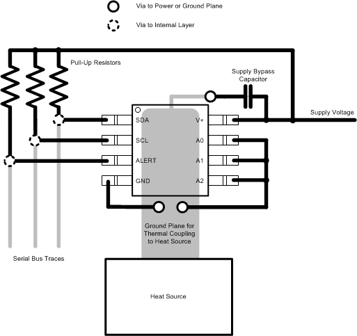
Mount the TMP275-Q1 to a PCB as shown in Figure 17. For this example the A0, A1, and A2 address pins are connected directly to ground. Connecting these pins to ground configures the device for slave address 1001000b.

  • Bypass the V+ pin to ground with a low-ESR ceramic bypass capacitor. The typical recommended bypass capacitance is a 0.1-μF ceramic capacitor with a X5R or X7R dielectric. The optimum placement is closest to the V+ and GND pins of the device. Take care in minimizing the loop area formed by the bypass-capacitor connection, the V+ pin, and the GND pin of the device. Additional bypass capacitance can be added to compensate for noisy or high-impedance power supplies.
  • Pull up the open-drain output pins SDA, SCL, and ALERT through 5-kΩ pullup resistors.

Layout Example

TMP275-Q1 ai_recommended_layout_sbos760.gif Figure 17. TMP275-Q1 Layout Example