SBOS363F June   2006  – May 2018 TMP275

PRODUCTION DATA.  

  1. Features
  2. Applications
  3. Description
    1.     Device Images
      1.      Simplified Schematic
      2.      Internal Block Diagram
  4. Revision History
  5. Pin Configuration and Functions
    1.     Pin Functions
  6. Specifications
    1. 6.1 Absolute Maximum Ratings
    2. 6.2 ESD Ratings
    3. 6.3 Recommended Operating Conditions
    4. 6.4 Thermal Information
    5. 6.5 Electrical Characteristics
    6. 6.6 Timing Requirements
    7. 6.7 Typical Characteristics
  7. Detailed Description
    1. 7.1 Overview
    2. 7.2 Functional Block Diagram
    3. 7.3 Feature Description
      1. 7.3.1 Digital Temperature Output
      2. 7.3.2 Serial Interface
      3. 7.3.3 Bus Overview
      4. 7.3.4 Serial Bus Address
        1. 7.3.4.1 Writing and Reading to the TMP275
        2. 7.3.4.2 Slave Mode Operations
          1. 7.3.4.2.1 Slave Receiver Mode
          2. 7.3.4.2.2 Slave Transmitter Mode
        3. 7.3.4.3 SMBus Alert Function
        4. 7.3.4.4 General Call
        5. 7.3.4.5 High-Speed Mode
        6. 7.3.4.6 Time-Out Function
      5. 7.3.5 Timing Diagrams
      6. 7.3.6 Two-Wire Timing Diagrams
    4. 7.4 Device Functional Modes
      1. 7.4.1 Shutdown Mode (SD)
      2. 7.4.2 Thermostat Mode (TM)
        1. 7.4.2.1 Comparator Mode (TM = 0)
        2. 7.4.2.2 Interrupt Mode (TM = 1)
      3. 7.4.3 One-Shot (OS)
    5. 7.5 Programming
      1. 7.5.1  Pointer Register
        1. 7.5.1.1 Pointer Register Byte (offset = N/A) [reset = 00h]
        2. 7.5.1.2 Pointer Addresses of the TMP275
          1. Table 3. Pointer Addresses of the TMP275 Field Description
      2. 7.5.2  Temperature Register
      3. 7.5.3  Configuration Register
      4. 7.5.4  Shutdown Mode (SD)
      5. 7.5.5  Thermostat Mode (TM)
      6. 7.5.6  Polarity (POL)
      7. 7.5.7  Fault Queue (F1/F0)
      8. 7.5.8  Converter Resolution (R1/R0)
      9. 7.5.9  One-Shot (OS)
      10. 7.5.10 High and Low Limit Registers
  8. Application and Implementation
    1. 8.1 Application Information
    2. 8.2 Typical Applications
      1. 8.2.1 Typical Connections of the TMP275
        1. 8.2.1.1 Design Requirements
        2. 8.2.1.2 Detailed Design Procedure
        3. 8.2.1.3 Application Curve
      2. 8.2.2 Connecting Multiple Devices on a Single Bus
      3. 8.2.3 Temperature Data Logger for Cold Chain Management Applications
  9. Power Supply Recommendations
  10. 10Layout
    1. 10.1 Layout Guidelines
    2. 10.2 Layout Example
  11. 11Device and Documentation Support
    1. 11.1 Documentation Support
      1. 11.1.1 Related Documentation
    2. 11.2 Community Resources
    3. 11.3 Trademarks
    4. 11.4 Electrostatic Discharge Caution
    5. 11.5 Glossary
  12. 12Mechanical, Packaging, and Orderable Information

Package Options

Mechanical Data (Package|Pins)
Thermal pad, mechanical data (Package|Pins)
Orderable Information

Two-Wire Timing Diagrams

TMP275 ai_tim_bus_bos448.gifFigure 7. Two-Wire Timing Diagram
TMP275 two_wire_tim_write_bos363d.gifFigure 8. Two-Wire Timing Diagram for TMP275 Write Word Format
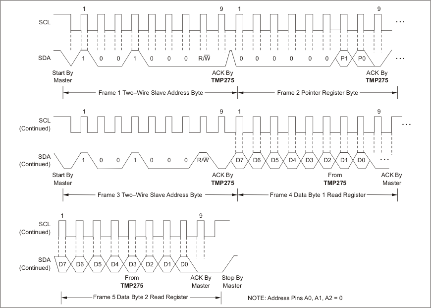
TMP275 two_wire_tim_read_bos363d.gifFigure 9. Two-Wire Timing Diagram for Read Word Format
TMP275 tim_SMBus_ALERT_bos363d.gifFigure 10. Timing Diagram for SMBus ALERT