SBOS335F June 2005 – January 2023 TMP300
PRODUCTION DATA
- 1Features
- 2Applications
- 3Description
- 4Revision History
- 5Pin Configuration and Functions
- 6Specifications
- 7Detailed Description
- 8Device and Documentation Support
- 9Mechanical, Packaging, and Orderable Information
Package Options
Mechanical Data (Package|Pins)
Thermal pad, mechanical data (Package|Pins)
Orderable Information
7.2.5 Hysteresis
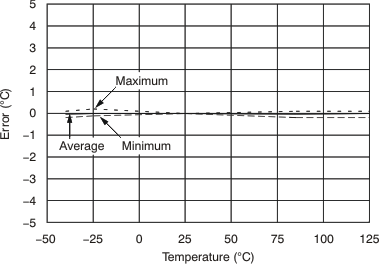
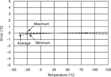
The hysteresis pin has two settings. Grounding HYSTSET results in 5°C of hysteresis. Connecting HYSTSET to VS results in 10°C of hysteresis. Figure 7-5 and Figure 7-6 show the hysteresis error variation over temperature.
 Figure 7-5 5°C Hysteresis Error vs Temperature
 Figure 7-6 10°C Hysteresis Error vs Temperature
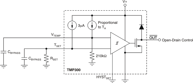
Use bypass capacitors on the supplies as well as on the RSET and analog out (VTEMP) pins when in noisy environments, as shown in Figure 7-7. These capacitors reduce premature triggering of the comparator.
 Figure 7-7 Bypass Capacitors Prevent Early Comparator Toggling Due to Circuit Board Noise