SBOS835C May 2017 – October 2019 TMP464
PRODUCTION DATA.
- 1 Features
- 2 Applications
- 3 Description
- 4 Revision History
- 5 Pin Configuration and Functions
- 6 Specifications
-
7 Detailed Description
- 7.1 Overview
- 7.2 Functional Block Diagram
- 7.3 Feature Description
- 7.4 Device Functional Modes
- 7.5 Programming
- 7.6
Register Maps
- 7.6.1
Register Information
- 7.6.1.1 Pointer Register
- 7.6.1.2 Local and Remote Temperature Value Registers
- 7.6.1.3 Software Reset Register
- 7.6.1.4 THERM Status Register
- 7.6.1.5 THERM2 Status Register
- 7.6.1.6 Remote Channel Open Status Register
- 7.6.1.7 Configuration Register
- 7.6.1.8 η-Factor Correction Register
- 7.6.1.9 Remote Temperature Offset Register
- 7.6.1.10 THERM Hysteresis Register
- 7.6.1.11 Local and Remote THERM and THERM2 Limit Registers
- 7.6.1.12 Block Read - Auto Increment Pointer
- 7.6.1.13 Lock Register
- 7.6.1.14 Manufacturer and Device Identification Plus Revision Registers
- 7.6.1
Register Information
- 8 Application and Implementation
- 9 Power Supply Recommendations
- 10Layout
- 11Device and Documentation Support
- 12Mechanical, Packaging, and Orderable Information
Package Options
Mechanical Data (Package|Pins)
- RGT|16
Thermal pad, mechanical data (Package|Pins)
- RGT|16
Orderable Information
7.5.1.2 Bus Definitions
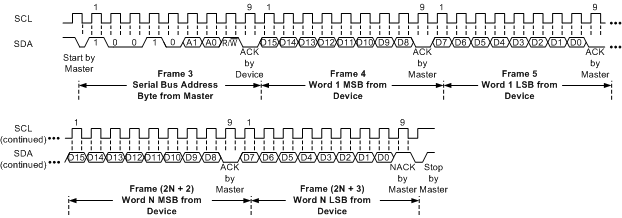
The TMP464 device has a two-wire interface that is compatible with the I2C or SMBus interface. Figure 13 through Figure 18 illustrate the timing for various operations on the TMP464 device. The bus definitions are as follows:
- Bus Idle:Both SDA and SCL lines remain high.
- Start Data Transfer:A change in the state of the SDA line (from high to low) when the SCL line is high defines a start condition. Each data transfer initiates with a start condition.
- Stop Data Transfer:A change in the state of the SDA line (from low to high) when the SCL line is high defines a stop condition. Each data transfer terminates with a repeated start or stop condition.
- Data Transfer:The number of data bytes transferred between a start and stop condition is not limited and is determined by the master device. The receiver acknowledges the data transfer.
- Acknowledge:Each receiving device, when addressed, is obliged to generate an acknowledge bit. A device that acknowledges must pull down the SDA line during the acknowledge clock pulse in such a way that the SDA line is stable low during the high period of the acknowledge clock pulse. Take setup and hold times into account. On a master receive, data transfer termination can be signaled by the master generating a not-acknowledge on the last byte that is transmitted by the slave.
 Figure 13. Two-Wire Timing Diagram for Write Pointer Byte
  Figure 14. Two-Wire Timing Diagram for Write Pointer Byte and Value Word
1. The master must leave SDA high to terminate a single-byte read operation.
Figure 15. Two-Wire Timing Diagram for Pointer Set Followed by a Repeat Start and Single-Byte Read Format  Figure 16. Two-Wire Timing Diagram for Pointer Byte Set Followed by a Repeat Start and Word (Two-Byte) Read
  Figure 17. Two-Wire Timing Diagram for Pointer Byte Set Followed by a Repeat Start and Multiple-Word (N-Word) Read
  Figure 18. Two-Wire Timing Diagram for Multiple-Word (N-Word) Read Without a Pointer Byte Set