SBOS759 November   2015 TMP175-Q1 , TMP75-Q1

PRODUCTION DATA.  

  1. Features
  2. Applications
  3. Description
  4. Revision History
  5. Pin Configuration and Functions
  6. Specifications
    1. 6.1 Absolute Maximum Ratings
    2. 6.2 ESD Ratings
    3. 6.3 Recommended Operating Conditions
    4. 6.4 Thermal Information
    5. 6.5 Electrical Characteristics
    6. 6.6 Timing Requirements
    7. 6.7 Typical Characteristics
  7. Detailed Description
    1. 7.1 Overview
    2. 7.2 Functional Block Diagram
    3. 7.3 Feature Description
      1. 7.3.1 Digital Temperature Output
      2. 7.3.2 Serial Interface
        1. 7.3.2.1 Bus Overview
        2. 7.3.2.2 Serial Bus Address
        3. 7.3.2.3 Writing and Reading to the TMP175-Q1 and TMP75-Q1
        4. 7.3.2.4 Slave Mode Operations
          1. 7.3.2.4.1 Slave Receiver Mode
          2. 7.3.2.4.2 Slave Transmitter Mode
        5. 7.3.2.5 SMBus Alert Function
        6. 7.3.2.6 General Call
        7. 7.3.2.7 High-Speed Mode
        8. 7.3.2.8 Time-out Function
      3. 7.3.3 Timing Diagrams
        1. 7.3.3.1 Two-Wire Timing Diagrams
    4. 7.4 Device Functional Modes
      1. 7.4.1 Shutdown Mode (SD)
      2. 7.4.2 One-Shot (OS)
      3. 7.4.3 Thermostat Mode (TM)
        1. 7.4.3.1 Comparator Mode (TM = 0)
        2. 7.4.3.2 Interrupt Mode (TM = 1)
    5. 7.5 Programming
      1. 7.5.1 Pointer Register
      2. 7.5.2 Temperature Register
      3. 7.5.3 Configuration Register
        1. 7.5.3.1 Polarity (POL)
        2. 7.5.3.2 Fault Queue (F1/F0)
        3. 7.5.3.3 Converter Resolution (R1/R0)
      4. 7.5.4 High- and Low-Limit Registers
  8. Application and Implementation
    1. 8.1 Application Information
    2. 8.2 Typical Application
      1. 8.2.1 Design Requirements
      2. 8.2.2 Detailed Design Procedure
      3. 8.2.3 Application Curve
  9. Power Supply Recommendations
  10. 10Layout
    1. 10.1 Layout Guidelines
    2. 10.2 Layout Example
  11. 11Device and Documentation Support
    1. 11.1 Related Links
    2. 11.2 Community Resources
    3. 11.3 Trademarks
    4. 11.4 Electrostatic Discharge Caution
    5. 11.5 Glossary
  12. 12Mechanical, Packaging, and Orderable Information

Package Options

Mechanical Data (Package|Pins)
Thermal pad, mechanical data (Package|Pins)
Orderable Information

5 Pin Configuration and Functions

DGK, D Packages
8-Pin VSSOP, SOIC
Top View
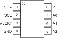
TMP175-Q1 TMP75-Q1 po_01_bos288j.gif
NOTE: Pin 1 is determined by orienting the package marking as indicated in the diagram.

Pin Functions

PIN I/O DESCRIPTION
NO. NAME
1 SDA I/O Serial data. Open-drain output; requires a pullup resistor.
2 SCL I Serial clock. Open-drain output; requires a pullup resistor.
3 ALERT O Overtemperature alert. Open-drain output; requires a pullup resistor.
4 GND Ground
5 A2 I Address select. Connect to GND, V+, or (for the TMP175-Q1 device only) leave these pins floating.
6 A1
7 A0
8 V+ I Supply voltage, 2.7 V to 5.5 V