SBOS721B October 2014 – October 2024 TMP75B-Q1
PRODUCTION DATA
- 1
- 1 Features
- 2 Applications
- 3 Description
- 4 Device Comparison
- 5 Pin Configuration and Functions
- 6 Specifications
-
7 Detailed Description
- 7.1 Overview
- 7.2 Functional Block Diagram
- 7.3
Feature Description
- 7.3.1 Digital Temperature Output
- 7.3.2 Temperature Limits and Alert
- 7.3.3 Serial Interface
- 7.4 Device Functional Modes
- 7.5 Programming
- 8 Register Map
- 9 Application and Implementation
- 10Device and Documentation Support
- 11Revision History
- 12Mechanical, Packaging, and Orderable Information
Package Options
Mechanical Data (Package|Pins)
Thermal pad, mechanical data (Package|Pins)
Orderable Information
3 Description
The TMP75B-Q1 is an integrated digital temperature sensor with a 12-bit analog-to-digital converter (ADC) that can operate at a 1.8V supply, and is pin and register compatible with the industry-standard LM75 and TMP75. This device is available in SOIC-8 and VSSOP-8 packages, and requires no external components to sense the temperature. The TMP75B-Q1 is capable of reading temperatures with a resolution of 0.0625°C with operating temperature range of –40°C to 125°C. The TMP75BTQDGKRQ1 is tri-temperature (–40°C, 25°C, and 125°C) tested in production for improved robustness.
The TMP75B-Q1 features SMBus and two-wire interface compatibility, and allows up to eight devices on the same bus with the SMBus overtemperature alert function. The programmable temperature limits and the ALERT pin allow the sensor to operate as a stand-alone thermostat, or an overtemperature alarm for power throttling or system shutdown. The factory-calibrated temperature accuracy and the noise-immune digital interface make the TMP75B-Q1 the preferred solution for temperature compensation of other sensors and electronic components. The TMP75B-Q1 is designed for thermal management and protection of a variety of automotive applications, and is a high-performance alternative to a PCB-mounted thermistor.
| DEVICE NAME | PACKAGE(1) | PACKAGE SIZE(2) |
|---|---|---|
|
TMP75BQDRQ1 | D (SOIC, 8) | 4.9mm × 6mm |
| TMP75BQDGKRQ1 | DGK (VSSOP, 8) | 3mm × 4.9mm |
TMP75BTQDGKRQ1 |
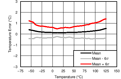
 Temperature Accuracy (Error) vs Ambient Temperature