SBOS721B October 2014 – October 2024 TMP75B-Q1
PRODUCTION DATA
- 1
- 1 Features
- 2 Applications
- 3 Description
- 4 Device Comparison
- 5 Pin Configuration and Functions
- 6 Specifications
-
7 Detailed Description
- 7.1 Overview
- 7.2 Functional Block Diagram
- 7.3
Feature Description
- 7.3.1 Digital Temperature Output
- 7.3.2 Temperature Limits and Alert
- 7.3.3 Serial Interface
- 7.4 Device Functional Modes
- 7.5 Programming
- 8 Register Map
- 9 Application and Implementation
- 10Device and Documentation Support
- 11Revision History
- 12Mechanical, Packaging, and Orderable Information
Package Options
Mechanical Data (Package|Pins)
Thermal pad, mechanical data (Package|Pins)
Orderable Information
7.4.1 Continuous-Conversion Mode
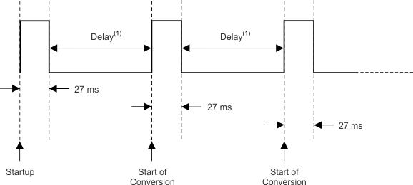
The default mode of the TMP75B-Q1 is continuous conversion, where the ADC performs continuous temperature conversions and stores each result to the temperature register, overwriting the result from the previous conversion. Conversion rate bits CR1 and CR0 in the configuration register configure the TMP75B-Q1 for typical conversion rates of 37Hz, 18Hz, 9Hz, or 4Hz. The TMP75B-Q1 has a typical conversion time of 27ms. To achieve different conversion rates, the TMP75B-Q1 makes a conversion, and then powers down and waits for the appropriate delay set by CR1 and CR0. The default rate is 37Hz (no delay between conversions).Table 7-3 shows the settings for CR1 and CR0.
| CR1 | CR0 | CONVERSION RATE (TYP) | IQ (TYP) |
|---|---|---|---|
| 0 | 0 | 37Hz (continuous conversion, default) | 45μA |
| 0 | 1 | 18Hz | 22μA |
| 1 | 0 | 9Hz | 12μA |
| 1 | 1 | 4Hz | 6.5μA |
After power-up or a general-call reset, the TMP75B-Q1 immediately starts a conversion, as shown in Figure 7-6. The first result is available after 27ms (typical). The active quiescent current during conversion is 45μA (typical at 25°C). The quiescent current during delay is 1μA (typical at 25°C).
