SBOS721B October 2014 – October 2024 TMP75B-Q1
PRODUCTION DATA
- 1
- 1 Features
- 2 Applications
- 3 Description
- 4 Device Comparison
- 5 Pin Configuration and Functions
- 6 Specifications
-
7 Detailed Description
- 7.1 Overview
- 7.2 Functional Block Diagram
- 7.3
Feature Description
- 7.3.1 Digital Temperature Output
- 7.3.2 Temperature Limits and Alert
- 7.3.3 Serial Interface
- 7.4 Device Functional Modes
- 7.5 Programming
- 8 Register Map
- 9 Application and Implementation
- 10Device and Documentation Support
- 11Revision History
- 12Mechanical, Packaging, and Orderable Information
Package Options
Mechanical Data (Package|Pins)
Thermal pad, mechanical data (Package|Pins)
Orderable Information
7.3.2 Temperature Limits and Alert
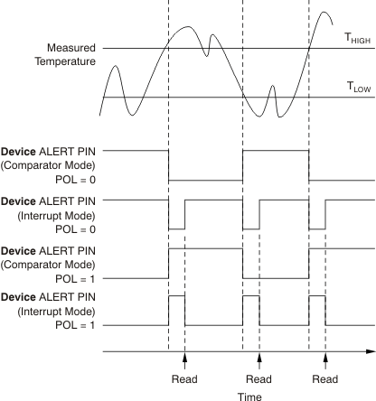
The temperature limits are stored in the TLOW and THIGH registers (Table 8-4 and Table 8-5) in the same format as the temperature result, and the values are compared to the temperature result on every conversion. The outcome of the comparison drives the behavior of the ALERT pin, which can operate as a comparator output or an interrupt, and is set by the TM bit in the configuration register (Table 8-3).
In comparator mode (TM = 0, default), the ALERT pin becomes active when the temperature is equal to or exceeds the value in THIGH (fault conditions) for a consecutive number of conversions as set by the FQ bits of the configuration register. ALERT clears when the temperature falls below TLOW for the same consecutive number of conversions. The difference between the two limits acts as a hysteresis on the comparator output, and a fault counter prevents false alerts as a result of environmental noise.
In interrupt mode (TM = 1), the ALERT pin becomes active when the temperature equals or exceeds the value in THIGH for a consecutive number of fault conditions. The ALERT pin remains active until a read operation of any register occurs, or the device successfully responds to the SMBus alert response address. The ALERT pin is also cleared if the device is placed in shutdown mode (see the Shutdown Mode section for shutdown mode description). After the ALERT pin is cleared, this pin becomes active again only when the temperature falls below TLOW for a consecutive number of fault conditions, and remains active until cleared by a read operation of any register, or a successful response to the SMBus alert response address. After the ALERT pin is cleared, the cycle repeats with the ALERT pin becoming active when the temperature equals or exceeds THIGH, and so on. The ALERT pin can also be cleared by resetting the device with the general-call reset command. This action also clears the state of the internal registers in the device and the fault counter memory, returning the device to comparator mode (TM = 0).
The active state of the ALERT pin is set by the POL bit in the configuration register. When POL = 0 (default), the ALERT pin is active low. When POL = 1, the ALERT pin is active high. The operation of the ALERT pin in various modes is shown in Figure 7-1.
 Figure 7-1 ALERT Pin Modes of
Operation