SLDS153B May 2009 – November 2015 TMP815
PRODUCTION DATA.
- 1 Features
- 2 Applications
- 3 Description
- 4 Revision History
- 5 Pin Configuration and Functions
- 6 Specifications
- 7 Detailed Description
- 8 Application and Implementation
- 9 Power Supply Recommendations
- 10Layout
- 11Device and Documentation Support
- 12Mechanical, Packaging, and Orderable Information
Package Options
Mechanical Data (Package|Pins)
- PW|16
Thermal pad, mechanical data (Package|Pins)
Orderable Information
7 Detailed Description
7.1 Overview
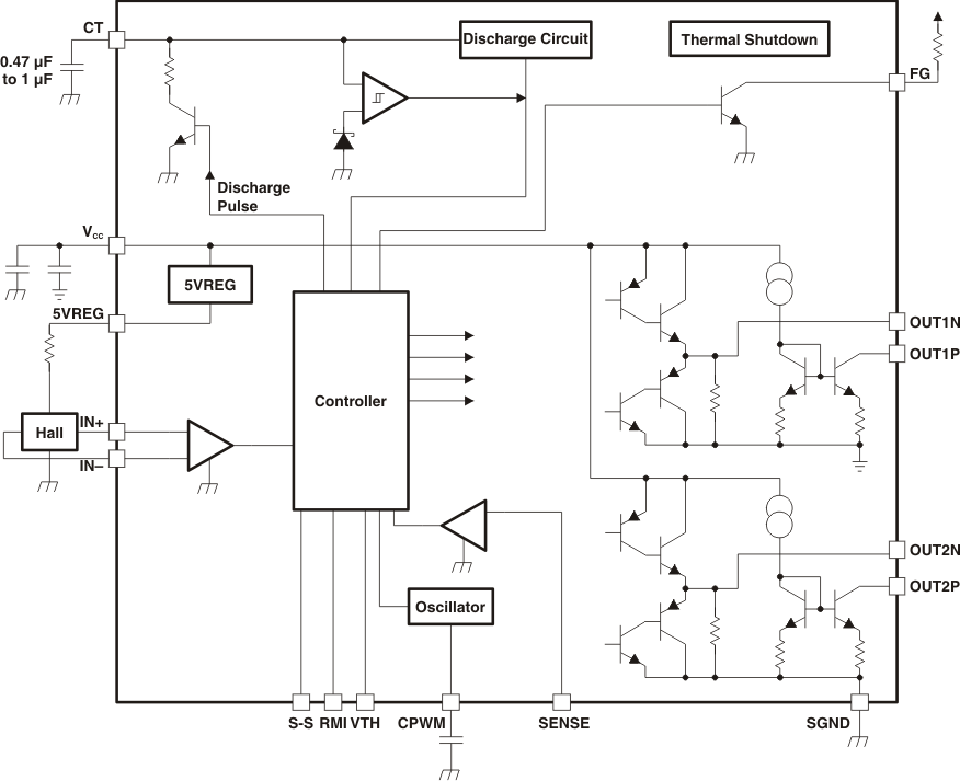
The TMP815 device is a single phase bipolar predriver which uses the hall sensor and speed control inputs for driving the single phase motor connected through the H Bridge. The predriver outputs are designed for driving top side P-channel and bottom side N-channel FETs in the bridge. Multiple protections like overcurrent, soft start, speed control, lock detect, speed feedback and minimum speed are incorporated in the device.
7.2 Functional Block Diagram

7.3 Feature Description
7.3.1 Speed Control
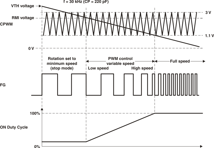
The speed control functionality is obtained by VTH pin of the device. For pulsed inputs, the user can supply a 20-kHz to 100-kHz frequency input (20 kHz to 50 kHz recommended) on the pin with a current limiting resistor in between.
If not used, this pin needs to be connected to ground for full speed.

7.3.2 Soft-Start
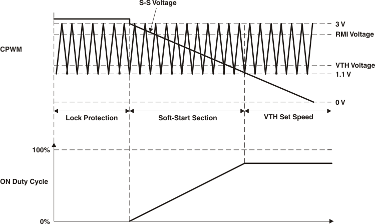
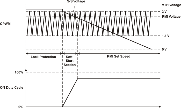
The speed control functionality is obtained by S-S pin of the device. Connection to the soft-start setting capacitor (see Figure 5) is through this pin. Connect the capacitor between S-S and 5VREG to set the soft-start time, according to the capacitance that is chosen (see Figure 3 and Figure 4). If the soft-start feature is not intended to be used, then the this pin needs to be connected to ground.


7.3.3 Lock Detection
When the rotor is locked by external means or load conditions, The lock detection feature helps to protect the circuit by not allowing the current to rise beyond control. A hiccup mechanism is also provided. The lock detection is enabled by a connection to the lock detection capacitor (see *10 in Figure 5) The constant current charge and discharge circuits cause drive stop when the pin voltage rises to 3 V and unlocking the drive when pin voltage falls to 1.1 V. If lock detection feature is not desired in the application, this pin needs to be connected to ground.
7.3.4 Current Limit
Current limit resistor is connected in a return path of H Bridge connection. This input is connected to the SENSE pin where the Current is limited when the voltage across this resistor crosses 200-mV threshold. The device enters in lower regeneration mode (see *8 in Figure 5) If not used, this pin needs to be connected to ground.
7.3.5 Minimum Speed Setting
Minimum speed setting (see *6 in Figure 5) feature is use with the RMI pin in the device. Connect to 5VREG with a pullup resistor if not used.
7.3.6 Speed Output
The speed of the motor while running can be observed at the FG pin which is an open collector output and needs to be pulled high for using it.
7.3.7 Drive Frequency Selection
The P channel switches in the device are switched with higher frequency whose duty cycle is decided by the speed control input. The frequency of the operation can be decided by the capacitor connected at the CPWM pin. As this is used also for the current limiting canceling signal, be sure to connect the capacitor even when speed control is not used.