SLDS153B May   2009  – November 2015 TMP815

PRODUCTION DATA.  

  1. Features
  2. Applications
  3. Description
  4. Revision History
  5. Pin Configuration and Functions
  6. Specifications
    1. 6.1 Absolute Maximum Ratings
    2. 6.2 ESD Ratings
    3. 6.3 Recommended Operating Conditions
    4. 6.4 Thermal Information
    5. 6.5 Electrical Characteristics
    6. 6.6 Typical Characteristics
  7. Detailed Description
    1. 7.1 Overview
    2. 7.2 Functional Block Diagram
    3. 7.3 Feature Description
      1. 7.3.1 Speed Control
      2. 7.3.2 Soft-Start
      3. 7.3.3 Lock Detection
      4. 7.3.4 Current Limit
      5. 7.3.5 Minimum Speed Setting
      6. 7.3.6 Speed Output
      7. 7.3.7 Drive Frequency Selection
    4. 7.4 Device Functional Modes
  8. Application and Implementation
    1. 8.1 Application Information
    2. 8.2 Typical Application
      1. 8.2.1 Design Requirements
      2. 8.2.2 Detailed Design Procedure
      3. 8.2.3 Application Curves
  9. Power Supply Recommendations
  10. 10Layout
    1. 10.1 Layout Guidelines
    2. 10.2 Layout Example
  11. 11Device and Documentation Support
    1. 11.1 Community Resource
    2. 11.2 Trademarks
    3. 11.3 Electrostatic Discharge Caution
    4. 11.4 Glossary
  12. 12Mechanical, Packaging, and Orderable Information

Package Options

Mechanical Data (Package|Pins)
Thermal pad, mechanical data (Package|Pins)
Orderable Information

10 Layout

10.1 Layout Guidelines

Connect 1-µF capacitor or greater between VCC and SGND with short traces.

Connect a capacitor between IN+ and IN- for noise reduction picked from Hall sensors.

Keep S-S, CT and CPWM capacitor near the device.

10.2 Layout Example
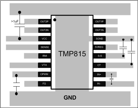
TMP815 lo_01_slds153.gif Figure 10. Recommended Layout Example