SPRS565D April 2009 – June 2014 TMS320C6743
PRODUCTION DATA.
- 1TMS320C6743 Fixed- and Floating-Point Digital Signal Processor
- 2Revision History
-
3Device Overview
- 3.1 Device Characteristics
- 3.2 Device Compatibility
- 3.3 DSP Subsystem
- 3.4 Memory Map Summary
- 3.5 Pin Assignments
- 3.6
Terminal Functions
- 3.6.1 Device Reset and JTAG
- 3.6.2 High-Frequency Oscillator and PLL
- 3.6.3 External Memory Interface A (ASYNC)
- 3.6.4 External Memory Interface B (SDRAM only)
- 3.6.5 Serial Peripheral Interface Modules (SPI0)
- 3.6.6 Enhanced Capture/Auxiliary PWM Modules (eCAP0, eCAP1, eCAP2)
- 3.6.7 Enhanced Pulse Width Modulators (eHRPWM0, eHRPWM1, eHRPWM2)
- 3.6.8 Enhanced Quadrature Encoder Pulse Module (eQEP)
- 3.6.9 Boot
- 3.6.10 Universal Asynchronous Receiver/Transmitters (UART0, UART2)
- 3.6.11 Inter-Integrated Circuit Modules (I2C0, I2C1)
- 3.6.12 Timers
- 3.6.13 Multichannel Audio Serial Ports (McASP0, McASP1)
- 3.6.14 Ethernet Media Access Controller (EMAC)
- 3.6.15 Multimedia Card/Secure Digital (MMC/SD)
- 3.6.16 General-Purpose IO Only Terminal Functions
- 3.6.17 Reserved and No Connect Terminal Functions
- 3.6.18 Supply and Ground Terminal Functions
- 4Device Configuration
-
5Device Operating Conditions
- 5.1 Absolute Maximum Ratings Over Operating Junction Temperature Range (Unless Otherwise Noted)
- 5.2 Handling Ratings
- 5.3 Recommended Operating Conditions
- 5.4 Notes on Recommended Power-On Hours (POH)
- 5.5 Electrical Characteristics Over Recommended Ranges of Supply Voltage and Operating Junction Temperature (Unless Otherwise Noted)
-
6Peripheral Information and Electrical Specifications
- 6.1 Parameter Information
- 6.2 Recommended Clock and Control Signal Transition Behavior
- 6.3 Power Supplies
- 6.4 Reset
- 6.5 Crystal Oscillator or External Clock Input
- 6.6 Clock PLLs
- 6.7 DSP Interrupts
- 6.8 General-Purpose Input/Output (GPIO)
- 6.9 EDMA
- 6.10 External Memory Interface A (EMIFA)
- 6.11 External Memory Interface B (EMIFB)
- 6.12 Memory Protection Units
- 6.13 MMC / SD / SDIO (MMCSD)
- 6.14 Ethernet Media Access Controller (EMAC)
- 6.15 Management Data Input/Output (MDIO)
- 6.16 Multichannel Audio Serial Ports (McASP0, McASP1)
- 6.17
Serial Peripheral Interface Ports (SPI0)
- 6.17.1 SPI Peripheral Registers Description(s)
- 6.17.2
SPI Electrical Data/Timing
- 6.17.2.1
Serial Peripheral Interface (SPI) Timing
- Table 6-49 General Timing Requirements for SPI0 Master Modes
- Table 6-50 General Timing Requirements for SPI0 Slave Modes
- Table 6-51 Additional SPI0 Master Timings, 4-Pin Enable Option
- Table 6-52 Additional SPI0 Master Timings, 4-Pin Chip Select Option
- Table 6-53 Additional SPI0 Master Timings, 5-Pin Option
- Table 6-54 Additional SPI0 Slave Timings, 4-Pin Enable Option
- Table 6-55 Additional SPI0 Slave Timings, 4-Pin Chip Select Option
- Table 6-56 Additional SPI0 Slave Timings, 5-Pin Option
- 6.17.2.1
Serial Peripheral Interface (SPI) Timing
- 6.18 Enhanced Capture (eCAP) Peripheral
- 6.19 Enhanced Quadrature Encoder (eQEP) Peripheral
- 6.20 Enhanced Pulse Width Modulator (eHRPWM) Modules
- 6.21 Timers
- 6.22 Inter-Integrated Circuit Serial Ports (I2C0, I2C1)
- 6.23 Universal Asynchronous Receiver/Transmitter (UART)
- 6.24 Power and Sleep Controller (PSC)
- 6.25 Programmable Real-Time Unit Subsystem (PRUSS)
- 6.26 Emulation Logic
- 6.27 IEEE 1149.1 JTAG
- 7Device and Documentation Support
- 8Mechanical Packaging and Orderable Information
Package Options
Refer to the PDF data sheet for device specific package drawings
Mechanical Data (Package|Pins)
- ZKB|256
- PTP|176
Thermal pad, mechanical data (Package|Pins)
- PTP|176
Orderable Information
Table 6-56 Additional(4) SPI0 Slave Timings, 5-Pin Option(1)(2)
| NO. | PARAMETER | MIN | MAX | UNIT | ||
|---|---|---|---|---|---|---|
| 25 | td(SCSL_SPC)S | Required delay from SPI0_SCS asserted at slave to first SPI0_CLK edge at slave. | 2P | ns | ||
| 26 | td(SPC_SCSH)S | Required delay from final SPI0_CLK edge before SPI0_SCS is deasserted. | Polarity = 0, Phase = 0,
from SPI0_CLK falling |
0.5tc(SPC)M + 5 | ns | |
| Polarity = 0, Phase = 1,
from SPI0_CLK falling |
5 | |||||
| Polarity = 1, Phase = 0,
from SPI0_CLK rising |
0.5tc(SPC)M + 5 | |||||
| Polarity = 1, Phase = 1,
from SPI0_CLK rising |
5 | |||||
| 27 | tena(SCSL_SOMI)S | Delay from master asserting SPI0_SCS to slave driving SPI0_SOMI valid | P + 18.5 | ns | ||
| 28 | tdis(SCSH_SOMI)S | Delay from master deasserting SPI0_SCS to slave 3-stating SPI0_SOMI | P + 18.5 | ns | ||
| 29 | tena(SCSL_ENA)S | Delay from master deasserting SPI0_SCS to slave driving SPI0_ENA valid | 18.5 | ns | ||
| 30 | tdis(SPC_ENA)S | Delay from final clock receive edge on SPI0_CLK to slave 3-stating or driving high SPI0_ENA.(3) | Polarity = 0, Phase = 0,
from SPI0_CLK falling |
2.5 P + 18.5 | ns | |
| Polarity = 0, Phase = 1,
from SPI0_CLK rising |
2.5 P + 18.5 | |||||
| Polarity = 1, Phase = 0,
from SPI0_CLK rising |
2.5 P + 18.5 | |||||
| Polarity = 1, Phase = 1,
from SPI0_CLK falling |
2.5 P + 18.5 | |||||
(1) P = SYSCLK2 period
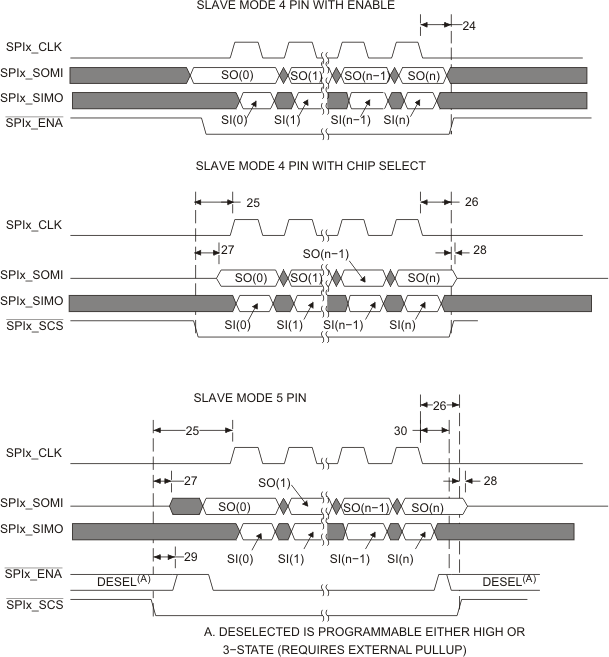
(2) Figure shows only Polarity = 0, Phase = 0 as an example. Table gives parameters for all four slave clocking modes.
(3) SPI0_ENA is driven low after the transmission completes if the SPIINT0.ENABLE_HIGHZ bit is programmed to 0. Otherwise it is tri-stated. If tri-stated, an external pullup resistor should be used to provide a valid level to the master. This option is useful when tying several SPI slave devices to a single master.
(4) These parameters are in addition to the general timings for SPI slave modes (Table 6-50).
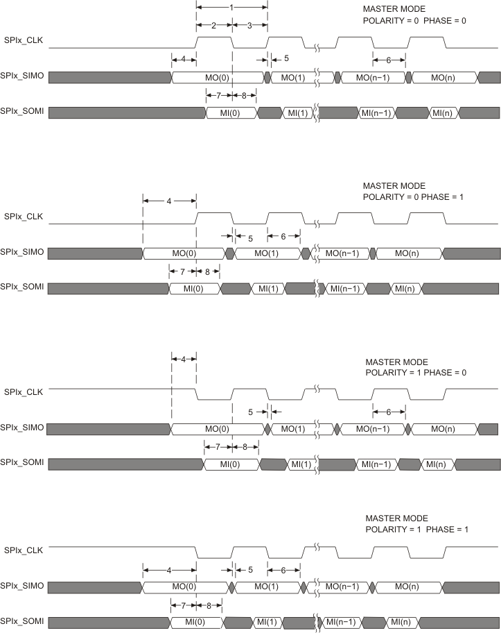
 Figure 6-33 SPI Timings—Master Mode
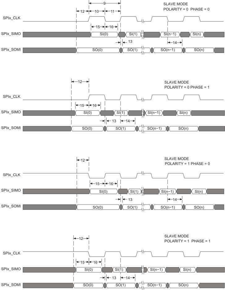
  Figure 6-34 SPI Timings—Slave Mode
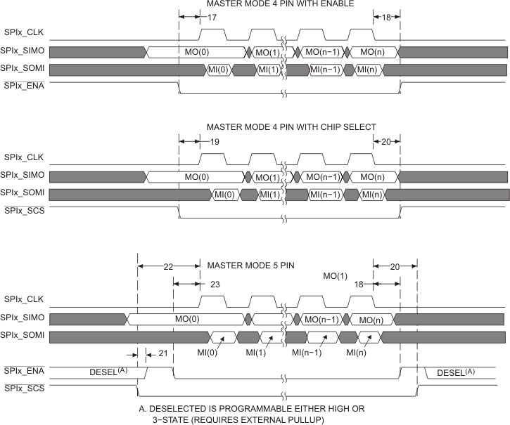
  Figure 6-35 SPI Timings—Master Mode (4-Pin and 5-Pin)
  Figure 6-36 SPI Timings—Slave Mode (4-Pin and 5-Pin)