SPRSP45C March 2020 – April 2024 TMS320F280021 , TMS320F280021-Q1 , TMS320F280023 , TMS320F280023-Q1 , TMS320F280023C , TMS320F280025 , TMS320F280025-Q1 , TMS320F280025C , TMS320F280025C-Q1
PRODUCTION DATA
- 1
- 1 Features
- 2 Applications
- 3 Description
- 4 Device Comparison
- 5 Terminal Configuration and Functions
-
6 Specifications
- 6.1 Absolute Maximum Ratings
- 6.2 ESD Ratings – Commercial
- 6.3 ESD Ratings – Automotive
- 6.4 Recommended Operating Conditions
- Supply Voltages
- 6.5 Power Consumption Summary
- 6.6 Electrical Characteristics
- 6.7 Thermal Resistance Characteristics for PN Package
- 6.8 Thermal Resistance Characteristics for PM Package
- 6.9 Thermal Resistance Characteristics for PT Package
- 6.10 Thermal Design Considerations
- 6.11
System
- 6.11.1 Power Management Module (PMM)
- 6.11.2 Reset Timing
- 6.11.3
Clock Specifications
- 6.11.3.1 Clock Sources
- 6.11.3.2 Clock Frequencies, Requirements, and Characteristics
- 6.11.3.3 Input Clocks and PLLs
- 6.11.3.4 XTAL Oscillator
- 6.11.3.5 Internal Oscillators
- 6.11.4 Flash Parameters
- 6.11.5 RAM Specifications
- 6.11.6 ROM Specifications
- 6.11.7 Emulation/JTAG
- 6.11.8 GPIO Electrical Data and Timing
- 6.11.9 Interrupts
- 6.11.10
Low-Power Modes
- 6.11.10.1 Clock-Gating Low-Power Modes
- 6.11.10.2
Low-Power Mode Wake-up Timing
- 6.11.10.2.1 IDLE Mode Timing Requirements
- 6.11.10.2.2 IDLE Mode Switching Characteristics
- 6.11.10.2.3 IDLE Entry and Exit Timing Diagram
- 6.11.10.2.4 STANDBY Mode Timing Requirements
- 6.11.10.2.5 STANDBY Mode Switching Characteristics
- 6.11.10.2.6 STANDBY Entry and Exit Timing Diagram
- 6.11.10.2.7 HALT Mode Timing Requirements
- 6.11.10.2.8 HALT Mode Switching Characteristics
- 6.11.10.2.9 HALT Entry and Exit Timing Diagram
- 6.12 Analog Peripherals
- 6.13
Control Peripherals
- 6.13.1 Enhanced Pulse Width Modulator (ePWM)
- 6.13.2 High-Resolution Pulse Width Modulator (HRPWM)
- 6.13.3 Enhanced Capture and High-Resolution Capture (eCAP, HRCAP)
- 6.13.4 Enhanced Quadrature Encoder Pulse (eQEP)
- 6.14
Communications Peripherals
- 6.14.1 Controller Area Network (CAN)
- 6.14.2 Inter-Integrated Circuit (I2C)
- 6.14.3 Power Management Bus (PMBus) Interface
- 6.14.4 Serial Communications Interface (SCI)
- 6.14.5 Serial Peripheral Interface (SPI)
- 6.14.6 Local Interconnect Network (LIN)
- 6.14.7 Fast Serial Interface (FSI)
- 6.14.8 Host Interface Controller (HIC)
-
7 Detailed Description
- 7.1 Overview
- 7.2 Functional Block Diagram
- 7.3 Memory
- 7.4 Identification
- 7.5 Bus Architecture – Peripheral Connectivity
- 7.6 C28x Processor
- 7.7 Embedded Real-Time Analysis and Diagnostic (ERAD)
- 7.8 Background CRC-32 (BGCRC)
- 7.9 Direct Memory Access (DMA)
- 7.10 Device Boot Modes
- 7.11 Dual Code Security Module
- 7.12 Watchdog
- 7.13 C28x Timers
- 7.14 Dual-Clock Comparator (DCC)
- 7.15 Configurable Logic Block (CLB)
- 8 Applications, Implementation, and Layout
- 9 Device and Documentation Support
- 10Revision History
- 11Mechanical, Packaging, and Orderable Information
Package Options
Mechanical Data (Package|Pins)
- PT|48
Thermal pad, mechanical data (Package|Pins)
Orderable Information
6.12.5 Comparator Subsystem (CMPSS)
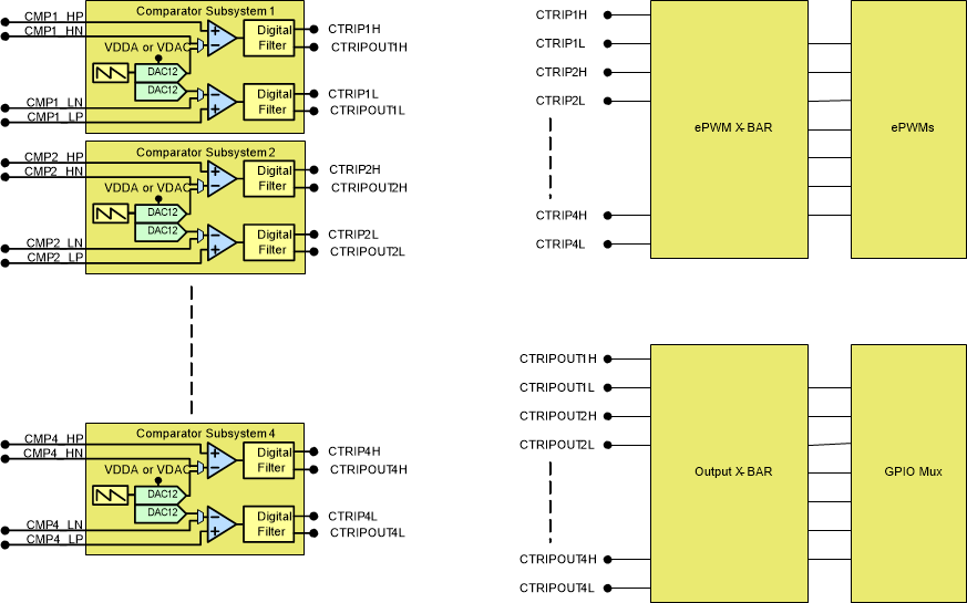
Each CMPSS contains two comparators, two reference 12-bit DACs, two digital filters, and one ramp generator. Comparators are denoted "H" or "L" within each module, where “H” and “L” represent high and low, respectively. Each comparator generates a digital output that indicates whether the voltage on the positive input is greater than the voltage on the negative input. The positive input of the comparator can be driven from an external pin or by the PGA . The negative input can be driven by an external pin or by the programmable reference 12-bit DAC. Each comparator output passes through a programmable digital filter that can remove spurious trip signals. An unfiltered output is also available if filtering is not required. A ramp generator circuit is optionally available to control the reference 12-bit DAC value for the high comparator in the subsystem. There are two outputs from each CMPSS module. These two outputs pass through the digital filters and crossbar before connecting to the ePWM modules or GPIO pin. Figure 6-44 shows the CMPSS connectivity.
For more information about the muxing of CMPSS pins, see the Analog Pins and Internal Connections table and the Pin Attributes table.
 Figure 6-44 CMPSS
Connectivity