SPRSP45C March 2020 – April 2024 TMS320F280021 , TMS320F280021-Q1 , TMS320F280023 , TMS320F280023-Q1 , TMS320F280023C , TMS320F280025 , TMS320F280025-Q1 , TMS320F280025C , TMS320F280025C-Q1
PRODUCTION DATA
- 1
- 1 Features
- 2 Applications
- 3 Description
- 4 Device Comparison
- 5 Terminal Configuration and Functions
-
6 Specifications
- 6.1 Absolute Maximum Ratings
- 6.2 ESD Ratings – Commercial
- 6.3 ESD Ratings – Automotive
- 6.4 Recommended Operating Conditions
- Supply Voltages
- 6.5 Power Consumption Summary
- 6.6 Electrical Characteristics
- 6.7 Thermal Resistance Characteristics for PN Package
- 6.8 Thermal Resistance Characteristics for PM Package
- 6.9 Thermal Resistance Characteristics for PT Package
- 6.10 Thermal Design Considerations
- 6.11
System
- 6.11.1 Power Management Module (PMM)
- 6.11.2 Reset Timing
- 6.11.3
Clock Specifications
- 6.11.3.1 Clock Sources
- 6.11.3.2 Clock Frequencies, Requirements, and Characteristics
- 6.11.3.3 Input Clocks and PLLs
- 6.11.3.4 XTAL Oscillator
- 6.11.3.5 Internal Oscillators
- 6.11.4 Flash Parameters
- 6.11.5 RAM Specifications
- 6.11.6 ROM Specifications
- 6.11.7 Emulation/JTAG
- 6.11.8 GPIO Electrical Data and Timing
- 6.11.9 Interrupts
- 6.11.10
Low-Power Modes
- 6.11.10.1 Clock-Gating Low-Power Modes
- 6.11.10.2
Low-Power Mode Wake-up Timing
- 6.11.10.2.1 IDLE Mode Timing Requirements
- 6.11.10.2.2 IDLE Mode Switching Characteristics
- 6.11.10.2.3 IDLE Entry and Exit Timing Diagram
- 6.11.10.2.4 STANDBY Mode Timing Requirements
- 6.11.10.2.5 STANDBY Mode Switching Characteristics
- 6.11.10.2.6 STANDBY Entry and Exit Timing Diagram
- 6.11.10.2.7 HALT Mode Timing Requirements
- 6.11.10.2.8 HALT Mode Switching Characteristics
- 6.11.10.2.9 HALT Entry and Exit Timing Diagram
- 6.12 Analog Peripherals
- 6.13
Control Peripherals
- 6.13.1 Enhanced Pulse Width Modulator (ePWM)
- 6.13.2 High-Resolution Pulse Width Modulator (HRPWM)
- 6.13.3 Enhanced Capture and High-Resolution Capture (eCAP, HRCAP)
- 6.13.4 Enhanced Quadrature Encoder Pulse (eQEP)
- 6.14
Communications Peripherals
- 6.14.1 Controller Area Network (CAN)
- 6.14.2 Inter-Integrated Circuit (I2C)
- 6.14.3 Power Management Bus (PMBus) Interface
- 6.14.4 Serial Communications Interface (SCI)
- 6.14.5 Serial Peripheral Interface (SPI)
- 6.14.6 Local Interconnect Network (LIN)
- 6.14.7 Fast Serial Interface (FSI)
- 6.14.8 Host Interface Controller (HIC)
-
7 Detailed Description
- 7.1 Overview
- 7.2 Functional Block Diagram
- 7.3 Memory
- 7.4 Identification
- 7.5 Bus Architecture – Peripheral Connectivity
- 7.6 C28x Processor
- 7.7 Embedded Real-Time Analysis and Diagnostic (ERAD)
- 7.8 Background CRC-32 (BGCRC)
- 7.9 Direct Memory Access (DMA)
- 7.10 Device Boot Modes
- 7.11 Dual Code Security Module
- 7.12 Watchdog
- 7.13 C28x Timers
- 7.14 Dual-Clock Comparator (DCC)
- 7.15 Configurable Logic Block (CLB)
- 8 Applications, Implementation, and Layout
- 9 Device and Documentation Support
- 10Revision History
- 11Mechanical, Packaging, and Orderable Information
Package Options
Mechanical Data (Package|Pins)
- PT|48
Thermal pad, mechanical data (Package|Pins)
Orderable Information
6.11.2 Reset Timing
XRSn is the device reset pin. It functions as an input and open-drain output. The device has a built-in power-on reset (POR). During power up, the POR circuit drives the XRSn pin low. A watchdog or NMI watchdog reset will also drive the pin low. An external open-drain circuit may drive the pin to assert a device reset.
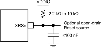
A resistor with a value from 2.2 kΩ to 10 kΩ should be placed between XRSn and VDDIO. A capacitor should be placed between XRSn and VSS for noise filtering, it should be 100 nF or smaller. These values will allow the watchdog to properly drive the XRSn pin to VOL within 512 OSCCLK cycles when the watchdog reset is asserted. Figure 6-10 shows the recommended reset circuit.
 Figure 6-10 Reset
Circuit