SPRSP45C March 2020 – April 2024 TMS320F280021 , TMS320F280021-Q1 , TMS320F280023 , TMS320F280023-Q1 , TMS320F280023C , TMS320F280025 , TMS320F280025-Q1 , TMS320F280025C , TMS320F280025C-Q1
PRODUCTION DATA
- 1
- 1 Features
- 2 Applications
- 3 Description
- 4 Device Comparison
- 5 Terminal Configuration and Functions
-
6 Specifications
- 6.1 Absolute Maximum Ratings
- 6.2 ESD Ratings – Commercial
- 6.3 ESD Ratings – Automotive
- 6.4 Recommended Operating Conditions
- Supply Voltages
- 6.5 Power Consumption Summary
- 6.6 Electrical Characteristics
- 6.7 Thermal Resistance Characteristics for PN Package
- 6.8 Thermal Resistance Characteristics for PM Package
- 6.9 Thermal Resistance Characteristics for PT Package
- 6.10 Thermal Design Considerations
- 6.11
System
- 6.11.1 Power Management Module (PMM)
- 6.11.2 Reset Timing
- 6.11.3
Clock Specifications
- 6.11.3.1 Clock Sources
- 6.11.3.2 Clock Frequencies, Requirements, and Characteristics
- 6.11.3.3 Input Clocks and PLLs
- 6.11.3.4 XTAL Oscillator
- 6.11.3.5 Internal Oscillators
- 6.11.4 Flash Parameters
- 6.11.5 RAM Specifications
- 6.11.6 ROM Specifications
- 6.11.7 Emulation/JTAG
- 6.11.8 GPIO Electrical Data and Timing
- 6.11.9 Interrupts
- 6.11.10
Low-Power Modes
- 6.11.10.1 Clock-Gating Low-Power Modes
- 6.11.10.2
Low-Power Mode Wake-up Timing
- 6.11.10.2.1 IDLE Mode Timing Requirements
- 6.11.10.2.2 IDLE Mode Switching Characteristics
- 6.11.10.2.3 IDLE Entry and Exit Timing Diagram
- 6.11.10.2.4 STANDBY Mode Timing Requirements
- 6.11.10.2.5 STANDBY Mode Switching Characteristics
- 6.11.10.2.6 STANDBY Entry and Exit Timing Diagram
- 6.11.10.2.7 HALT Mode Timing Requirements
- 6.11.10.2.8 HALT Mode Switching Characteristics
- 6.11.10.2.9 HALT Entry and Exit Timing Diagram
- 6.12 Analog Peripherals
- 6.13
Control Peripherals
- 6.13.1 Enhanced Pulse Width Modulator (ePWM)
- 6.13.2 High-Resolution Pulse Width Modulator (HRPWM)
- 6.13.3 Enhanced Capture and High-Resolution Capture (eCAP, HRCAP)
- 6.13.4 Enhanced Quadrature Encoder Pulse (eQEP)
- 6.14
Communications Peripherals
- 6.14.1 Controller Area Network (CAN)
- 6.14.2 Inter-Integrated Circuit (I2C)
- 6.14.3 Power Management Bus (PMBus) Interface
- 6.14.4 Serial Communications Interface (SCI)
- 6.14.5 Serial Peripheral Interface (SPI)
- 6.14.6 Local Interconnect Network (LIN)
- 6.14.7 Fast Serial Interface (FSI)
- 6.14.8 Host Interface Controller (HIC)
-
7 Detailed Description
- 7.1 Overview
- 7.2 Functional Block Diagram
- 7.3 Memory
- 7.4 Identification
- 7.5 Bus Architecture – Peripheral Connectivity
- 7.6 C28x Processor
- 7.7 Embedded Real-Time Analysis and Diagnostic (ERAD)
- 7.8 Background CRC-32 (BGCRC)
- 7.9 Direct Memory Access (DMA)
- 7.10 Device Boot Modes
- 7.11 Dual Code Security Module
- 7.12 Watchdog
- 7.13 C28x Timers
- 7.14 Dual-Clock Comparator (DCC)
- 7.15 Configurable Logic Block (CLB)
- 8 Applications, Implementation, and Layout
- 9 Device and Documentation Support
- 10Revision History
- 11Mechanical, Packaging, and Orderable Information
Package Options
Mechanical Data (Package|Pins)
Thermal pad, mechanical data (Package|Pins)
Orderable Information
6.14.7.2 FSI Receiver
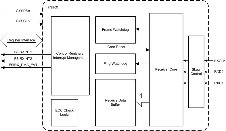
The receiver module interfaces to the FSI clock (RXCLK), and data lines (RXD0 and RXD1) after they pass through an optional programmable delay line. The receiver core handles the data framing, CRC computation, and frame-related error checking. The receiver bit clock and state machine are run by the RXCLK input, which is asynchronous to the device system clock.
The receiver control registers let the CPU program, control, and monitor the operation of the FSIRX. The receive data buffer is accessible by the CPU, HIC, and the DMA.
The receiver core has the following features:
- 16-word data buffer
- Multiple supported frame types
- Ping frame watchdog
- Frame watchdog
- CRC calculation and comparison in hardware
- ECC detection
- Programmable delay line control on incoming signals
- DMA support
- SPI compatibility mode
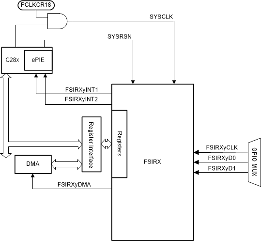
Figure 6-74 shows the FSIRX CPU interface. Figure 6-75 provides a high-level overview of the internal modules present in the FSIRX. Not all data paths and internal connections are shown.
 Figure 6-74 FSIRX CPU Interface
 Figure 6-75 FSIRX Block Diagram