SPRS945G January   2017  – January 2023 TMS320F280040-Q1 , TMS320F280040C-Q1 , TMS320F280041 , TMS320F280041-Q1 , TMS320F280041C , TMS320F280041C-Q1 , TMS320F280045 , TMS320F280048-Q1 , TMS320F280048C-Q1 , TMS320F280049 , TMS320F280049-Q1 , TMS320F280049C , TMS320F280049C-Q1

PRODUCTION DATA  

  1. Features
  2. Applications
  3. Description
    1. 3.1 Functional Block Diagram
  4. Revision History
  5. Device Comparison
    1. 5.1 Related Products
  6. Pin Configuration and Functions
    1. 6.1 Pin Diagrams
    2. 6.2 Pin Attributes
    3. 6.3 Signal Descriptions
      1. 6.3.1 Analog Signals
      2. 6.3.2 Digital Signals
      3. 6.3.3 Power and Ground
      4. 6.3.4 Test, JTAG, and Reset
    4. 6.4 Pin Multiplexing
      1. 6.4.1 GPIO Muxed Pins
      2. 6.4.2 Digital Inputs on ADC Pins (AIOs)
      3. 6.4.3 GPIO Input X-BAR
      4. 6.4.4 GPIO Output X-BAR and ePWM X-BAR
    5. 6.5 Pins With Internal Pullup and Pulldown
    6. 6.6 Connections for Unused Pins
  7. Specifications
    1. 7.1  Absolute Maximum Ratings
    2. 7.2  ESD Ratings – Commercial
    3. 7.3  ESD Ratings – Automotive
    4. 7.4  Recommended Operating Conditions
    5. 7.5  Power Consumption Summary
      1. 7.5.1 System Current Consumption (External Supply)
      2. 7.5.2 System Current Consumption (Internal VREG)
      3. 7.5.3 System Current Consumption (DCDC)
      4. 7.5.4 Operating Mode Test Description
      5. 7.5.5 Current Consumption Graphs
      6. 7.5.6 Reducing Current Consumption
        1. 7.5.6.1 Typical IDD Current Reduction per Disabled Peripheral (at 100-MHz SYSCLK)
    6. 7.6  Electrical Characteristics
    7. 7.7  Thermal Resistance Characteristics
      1. 7.7.1 PZ Package
      2. 7.7.2 PM Package
      3. 7.7.3 RSH Package
    8. 7.8  Thermal Design Considerations
    9. 7.9  System
      1. 7.9.1 Power Management Module (PMM)
        1. 7.9.1.1 Introduction
        2. 7.9.1.2 Overview
          1. 7.9.1.2.1 Power Rail Monitors
            1. 7.9.1.2.1.1 I/O POR (Power-On Reset) Monitor
            2. 7.9.1.2.1.2 I/O BOR (Brown-Out Reset) Monitor
            3. 7.9.1.2.1.3 VDD POR (Power-On Reset) Monitor
          2. 7.9.1.2.2 External Supervisor Usage
          3. 7.9.1.2.3 Delay Blocks
          4. 7.9.1.2.4 Internal 1.2-V LDO Voltage Regulator (VREG)
          5. 7.9.1.2.5 VREGENZ
          6. 7.9.1.2.6 Internal 1.2-V Switching Regulator (DC-DC)
            1. 7.9.1.2.6.1 PCB Layout and Component Guidelines
        3. 7.9.1.3 External Components
          1. 7.9.1.3.1 Decoupling Capacitors
            1. 7.9.1.3.1.1 VDDIO Decoupling
            2. 7.9.1.3.1.2 VDD Decoupling
        4. 7.9.1.4 Power Sequencing
          1. 7.9.1.4.1 Supply Pins Ganging
          2. 7.9.1.4.2 Signal Pins Power Sequence
          3. 7.9.1.4.3 Supply Pins Power Sequence
            1. 7.9.1.4.3.1 External VREG/VDD Mode Sequence
            2. 7.9.1.4.3.2 Internal VREG/VDD Mode Sequence
            3. 7.9.1.4.3.3 Supply Sequencing Summary and Effects of Violations
            4. 7.9.1.4.3.4 Supply Slew Rate
        5. 7.9.1.5 Power Management Module Electrical Data and Timing
          1. 7.9.1.5.1 Power Management Module Operating Conditions
          2. 7.9.1.5.2 Power Management Module Characteristics
          3.        Supply Voltages
      2. 7.9.2 Reset Timing
        1. 7.9.2.1 Reset Sources
        2. 7.9.2.2 Reset Electrical Data and Timing
          1. 7.9.2.2.1 Reset (XRSn) Timing Requirements
          2. 7.9.2.2.2 Reset (XRSn) Switching Characteristics
          3. 7.9.2.2.3 Reset Timing Diagram
      3. 7.9.3 Clock Specifications
        1. 7.9.3.1 Clock Sources
        2. 7.9.3.2 Clock Frequencies, Requirements, and Characteristics
          1. 7.9.3.2.1 Input Clock Frequency and Timing Requirements, PLL Lock Times
            1. 7.9.3.2.1.1 Input Clock Frequency
            2. 7.9.3.2.1.2 XTAL Oscillator Characteristics
            3. 7.9.3.2.1.3 X1 Timing Requirements
            4. 7.9.3.2.1.4 PLL Lock Times
          2. 7.9.3.2.2 Internal Clock Frequencies
            1. 7.9.3.2.2.1 Internal Clock Frequencies
          3. 7.9.3.2.3 Output Clock Frequency and Switching Characteristics
            1. 7.9.3.2.3.1 XCLKOUT Switching Characteristics
        3. 7.9.3.3 Input Clocks and PLLs
        4. 7.9.3.4 Crystal (XTAL) Oscillator
          1. 7.9.3.4.1 Introduction
          2. 7.9.3.4.2 Overview
            1. 7.9.3.4.2.1 Electrical Oscillator
              1. 7.9.3.4.2.1.1 Modes of Operation
                1. 7.9.3.4.2.1.1.1 Crystal Mode of Operation
                2. 7.9.3.4.2.1.1.2 Single-Ended Mode of Operation
              2. 7.9.3.4.2.1.2 XTAL Output on XCLKOUT
            2. 7.9.3.4.2.2 Quartz Crystal
            3. 7.9.3.4.2.3 GPIO Modes of Operation
          3. 7.9.3.4.3 Functional Operation
            1. 7.9.3.4.3.1 ESR – Effective Series Resistance
            2. 7.9.3.4.3.2 Rneg – Negative Resistance
            3. 7.9.3.4.3.3 Start-up Time
            4. 7.9.3.4.3.4 DL – Drive Level
          4. 7.9.3.4.4 How to Choose a Crystal
          5. 7.9.3.4.5 Testing
          6. 7.9.3.4.6 Common Problems and Debug Tips
          7. 7.9.3.4.7 Crystal Oscillator Specifications
            1. 7.9.3.4.7.1 Crystal Oscillator Parameters
            2. 7.9.3.4.7.2 Crystal Equivalent Series Resistance (ESR) Requirements
            3. 7.9.3.4.7.3 Crystal Oscillator Electrical Characteristics
        5. 7.9.3.5 Internal Oscillators
          1. 7.9.3.5.1 INTOSC Characteristics
      4. 7.9.4 Flash Parameters
      5. 7.9.5 Emulation/JTAG
        1. 7.9.5.1 JTAG Electrical Data and Timing
          1. 7.9.5.1.1 JTAG Timing Requirements
          2. 7.9.5.1.2 JTAG Switching Characteristics
          3. 7.9.5.1.3 JTAG Timing Diagram
        2. 7.9.5.2 cJTAG Electrical Data and Timing
          1. 7.9.5.2.1 cJTAG Timing Requirements
          2. 7.9.5.2.2 cJTAG Switching Characteristics
          3. 7.9.5.2.3 cJTAG Timing Diagram
      6. 7.9.6 GPIO Electrical Data and Timing
        1. 7.9.6.1 GPIO – Output Timing
          1. 7.9.6.1.1 General-Purpose Output Switching Characteristics
        2. 7.9.6.2 GPIO – Input Timing
          1. 7.9.6.2.1 General-Purpose Input Timing Requirements
        3. 7.9.6.3 Sampling Window Width for Input Signals
      7. 7.9.7 Interrupts
        1. 7.9.7.1 External Interrupt (XINT) Electrical Data and Timing
          1. 7.9.7.1.1 External Interrupt Timing Requirements
          2. 7.9.7.1.2 External Interrupt Switching Characteristics
          3. 7.9.7.1.3 Interrupt Timing Diagram
      8. 7.9.8 Low-Power Modes
        1. 7.9.8.1 Clock-Gating Low-Power Modes
        2. 7.9.8.2 Low-Power Mode Wake-up Timing
          1. 7.9.8.2.1 IDLE Mode Timing Requirements
          2. 7.9.8.2.2 IDLE Mode Switching Characteristics
          3. 7.9.8.2.3 IDLE Mode Timing Diagram
          4. 7.9.8.2.4 HALT Mode Timing Requirements
          5. 7.9.8.2.5 HALT Mode Switching Characteristics
          6. 7.9.8.2.6 HALT Mode Timing Diagram
    10. 7.10 Analog Peripherals
      1. 7.10.1 Analog-to-Digital Converter (ADC)
        1. 7.10.1.1 Result Register Mapping
        2. 7.10.1.2 ADC Configurability
          1. 7.10.1.2.1 Signal Mode
        3. 7.10.1.3 ADC Electrical Data and Timing
          1. 7.10.1.3.1 ADC Operating Conditions
          2. 7.10.1.3.2 ADC Characteristics
          3. 7.10.1.3.3 ADC Input Model
          4. 7.10.1.3.4 ADC Timing Diagrams
      2. 7.10.2 Programmable Gain Amplifier (PGA)
        1. 7.10.2.1 PGA Electrical Data and Timing
          1. 7.10.2.1.1 PGA Operating Conditions
          2. 7.10.2.1.2 PGA Characteristics
          3. 7.10.2.1.3 PGA Typical Characteristics Graphs
      3. 7.10.3 Temperature Sensor
        1. 7.10.3.1 Temperature Sensor Electrical Data and Timing
          1. 7.10.3.1.1 Temperature Sensor Characteristics
      4. 7.10.4 Buffered Digital-to-Analog Converter (DAC)
        1. 7.10.4.1 Buffered DAC Electrical Data and Timing
          1. 7.10.4.1.1 Buffered DAC Operating Conditions
          2. 7.10.4.1.2 Buffered DAC Electrical Characteristics
          3. 7.10.4.1.3 Buffered DAC Illustrative Graphs
          4. 7.10.4.1.4 Buffered DAC Typical Characteristics Graphs
      5. 7.10.5 Comparator Subsystem (CMPSS)
        1. 7.10.5.1 CMPSS Electrical Data and Timing
          1. 7.10.5.1.1 Comparator Electrical Characteristics
          2. 7.10.5.1.2 CMPSS DAC Static Electrical Characteristics
          3. 7.10.5.1.3 CMPSS Illustrative Graphs
    11. 7.11 Control Peripherals
      1. 7.11.1 Enhanced Capture (eCAP)
        1. 7.11.1.1 eCAP Electrical Data and Timing
          1. 7.11.1.1.1 eCAP Timing Requirements
          2. 7.11.1.1.2 eCAP Switching Characteristics
      2. 7.11.2 High-Resolution Capture Submodule (HRCAP6–HRCAP7)
        1. 7.11.2.1 HRCAP Electrical Data and Timing
          1. 7.11.2.1.1 HRCAP Switching Characteristics
      3. 7.11.3 Enhanced Pulse Width Modulator (ePWM)
        1. 7.11.3.1 Control Peripherals Synchronization
        2. 7.11.3.2 ePWM Electrical Data and Timing
          1. 7.11.3.2.1 ePWM Timing Requirements
          2. 7.11.3.2.2 ePWM Switching Characteristics
          3. 7.11.3.2.3 Trip-Zone Input Timing
            1. 7.11.3.2.3.1 Trip-Zone Input Timing Requirements
        3. 7.11.3.3 External ADC Start-of-Conversion Electrical Data and Timing
          1. 7.11.3.3.1 External ADC Start-of-Conversion Switching Characteristics
      4. 7.11.4 High-Resolution Pulse Width Modulator (HRPWM)
        1. 7.11.4.1 HRPWM Electrical Data and Timing
          1. 7.11.4.1.1 High-Resolution PWM Characteristics
      5. 7.11.5 Enhanced Quadrature Encoder Pulse (eQEP)
        1. 7.11.5.1 eQEP Electrical Data and Timing
          1. 7.11.5.1.1 eQEP Timing Requirements
          2. 7.11.5.1.2 eQEP Switching Characteristics
      6. 7.11.6 Sigma-Delta Filter Module (SDFM)
        1. 7.11.6.1 SDFM Electrical Data and Timing
          1. 7.11.6.1.1 SDFM Timing Requirements When Using Asynchronous GPIO (ASYNC) Option
          2. 7.11.6.1.2 SDFM Timing Diagram
        2. 7.11.6.2 SDFM Electrical Data and Timing (Synchronized GPIO)
          1. 7.11.6.2.1 SDFM Timing Requirements When Using Synchronized GPIO (SYNC) Option
    12. 7.12 Communications Peripherals
      1. 7.12.1 Controller Area Network (CAN)
      2. 7.12.2 Inter-Integrated Circuit (I2C)
        1. 7.12.2.1 I2C Electrical Data and Timing
          1. 7.12.2.1.1 I2C Timing Requirements
          2. 7.12.2.1.2 I2C Switching Characteristics
          3. 7.12.2.1.3 I2C Timing Diagram
      3. 7.12.3 Power Management Bus (PMBus) Interface
        1. 7.12.3.1 PMBus Electrical Data and Timing
          1. 7.12.3.1.1 PMBus Electrical Characteristics
          2. 7.12.3.1.2 PMBus Fast Mode Switching Characteristics
          3. 7.12.3.1.3 PMBus Standard Mode Switching Characteristics
      4. 7.12.4 Serial Communications Interface (SCI)
      5. 7.12.5 Serial Peripheral Interface (SPI)
        1. 7.12.5.1 SPI Electrical Data and Timing
          1. 7.12.5.1.1 Non-High-Speed Master Mode Timings
            1. 7.12.5.1.1.1 SPI Master Mode Switching Characteristics (Clock Phase = 0)
            2. 7.12.5.1.1.2 SPI Master Mode Switching Characteristics (Clock Phase = 1)
            3. 7.12.5.1.1.3 SPI Master Mode Timing Requirements
          2. 7.12.5.1.2 Non-High-Speed Slave Mode Timings
            1. 7.12.5.1.2.1 SPI Slave Mode Switching Characteristics
            2. 7.12.5.1.2.2 SPI Slave Mode Timing Requirements
          3. 7.12.5.1.3 High-Speed Master Mode Timings
            1. 7.12.5.1.3.1 SPI High-Speed Master Mode Switching Characteristics (Clock Phase = 0)
            2. 7.12.5.1.3.2 SPI High-Speed Master Mode Switching Characteristics (Clock Phase = 1)
            3. 7.12.5.1.3.3 SPI High-Speed Master Mode Timing Requirements
          4. 7.12.5.1.4 High-Speed Slave Mode Timings
            1. 7.12.5.1.4.1 SPI High-Speed Slave Mode Switching Characteristics
            2. 7.12.5.1.4.2 SPI High-Speed Slave Mode Timing Requirements
      6. 7.12.6 Local Interconnect Network (LIN)
      7. 7.12.7 Fast Serial Interface (FSI)
        1. 7.12.7.1 FSI Transmitter
          1. 7.12.7.1.1 FSITX Electrical Data and Timing
            1. 7.12.7.1.1.1 FSITX Switching Characteristics
        2. 7.12.7.2 FSI Receiver
          1. 7.12.7.2.1 FSIRX Electrical Data and Timing
            1. 7.12.7.2.1.1 FSIRX Switching Characteristics
            2. 7.12.7.2.1.2 FSIRX Timing Requirements
        3. 7.12.7.3 FSI SPI Compatibility Mode
          1. 7.12.7.3.1 FSITX SPI Signaling Mode Electrical Data and Timing
            1. 7.12.7.3.1.1 FSITX SPI Signaling Mode Switching Characteristics
  8. Detailed Description
    1. 8.1  Overview
    2. 8.2  Functional Block Diagram
    3. 8.3  Memory
      1. 8.3.1 C28x Memory Map
      2. 8.3.2 Control Law Accelerator (CLA) ROM Memory Map
      3. 8.3.3 Flash Memory Map
      4. 8.3.4 Peripheral Registers Memory Map
      5. 8.3.5 Memory Types
        1. 8.3.5.1 Dedicated RAM (Mx RAM)
        2. 8.3.5.2 Local Shared RAM (LSx RAM)
        3. 8.3.5.3 Global Shared RAM (GSx RAM)
        4. 8.3.5.4 CLA Message RAM (CLA MSGRAM)
    4. 8.4  Identification
    5. 8.5  Bus Architecture – Peripheral Connectivity
    6. 8.6  C28x Processor
      1. 8.6.1 Embedded Real-Time Analysis and Diagnostic (ERAD)
      2. 8.6.2 Floating-Point Unit (FPU)
      3. 8.6.3 Trigonometric Math Unit (TMU)
      4. 8.6.4 Viterbi, Complex Math and CRC Unit (VCU-I)
    7. 8.7  Control Law Accelerator (CLA)
    8. 8.8  Direct Memory Access (DMA)
    9. 8.9  Boot ROM and Peripheral Booting
      1. 8.9.1 Configuring Alternate Boot Mode Select Pins
      2. 8.9.2 Configuring Alternate Boot Mode Options
      3. 8.9.3 GPIO Assignments
    10. 8.10 Dual Code Security Module
    11. 8.11 Watchdog
    12. 8.12 Configurable Logic Block (CLB)
    13. 8.13 Functional Safety
  9. Applications, Implementation, and Layout
    1. 9.1 Key Device Features
    2. 9.2 Application Information
      1. 9.2.1 Typical Application
        1. 9.2.1.1 Server Telecom Power Supply Unit (PSU)
          1. 9.2.1.1.1 System Block Diagram
          2. 9.2.1.1.2 Server and Telecom PSU Resources
        2. 9.2.1.2 Single-Phase Online UPS
          1. 9.2.1.2.1 System Block Diagram
          2. 9.2.1.2.2 Single phase online UPS Resources
        3. 9.2.1.3 Solar Micro Inverter
          1. 9.2.1.3.1 System Block Diagram
          2. 9.2.1.3.2 Solar Micro Inverter Resources
        4. 9.2.1.4 EV Charging Station Power Module
          1. 9.2.1.4.1 System Block Diagram
          2. 9.2.1.4.2 EV charging station power module Resources
        5. 9.2.1.5 Servo Drive Control Module
          1. 9.2.1.5.1 System Block Diagram
          2. 9.2.1.5.2 Servo Drive Control Module Resources
  10. 10Device and Documentation Support
    1. 10.1 Device and Development Support Tool Nomenclature
    2. 10.2 Markings
    3. 10.3 Tools and Software
    4. 10.4 Documentation Support
    5. 10.5 Support Resources
    6. 10.6 Trademarks
    7. 10.7 Electrostatic Discharge Caution
    8. 10.8 Glossary
  11. 11Mechanical, Packaging, and Orderable Information
    1. 11.1 Packaging Information

Package Options

Mechanical Data (Package|Pins)
Thermal pad, mechanical data (Package|Pins)
Orderable Information

Device and Development Support Tool Nomenclature

To designate the stages in the product development cycle, TI assigns prefixes to the part numbers of all TMS320 MCU devices and support tools. Each TMS320™ MCU commercial family member has one of three prefixes: TMX, TMP, or TMS (for example, TMS320F280049). Texas Instruments recommends two of three possible prefix designators for its support tools: TMDX and TMDS. These prefixes represent evolutionary stages of product development from engineering prototypes (with TMX for devices and TMDX for tools) through fully qualified production devices and tools (with TMS for devices and TMDS for tools).

Device development evolutionary flow:

    TMX Experimental device that is not necessarily representative of the final device's electrical specifications and may not use production assembly flow.
    TMP Prototype device that is not necessarily the final silicon die and may not necessarily meet final electrical specifications.
    TMS Production version of the silicon die that is fully qualified.

Support tool development evolutionary flow:

    TMDX Development-support product that has not yet completed Texas Instruments internal qualification testing.
    TMDS Fully-qualified development-support product.

TMX and TMP devices and TMDX development-support tools are shipped against the following disclaimer:

"Developmental product is intended for internal evaluation purposes."

Production devices and TMDS development-support tools have been characterized fully, and the quality and reliability of the device have been demonstrated fully. TI's standard warranty applies.

Predictions show that prototype devices (X or P) have a greater failure rate than the standard production devices. Texas Instruments recommends that these devices not be used in any production system because their expected end-use failure rate still is undefined. Only qualified production devices are to be used.

TI device nomenclature also includes a suffix with the device family name. This suffix indicates the package type (for example, PZ) and temperature range (for example, S).

For device part numbers and further ordering information, see the TI website (www.ti.com) or contact your TI sales representative.

For additional description of the device nomenclature markings on the die, see the TMS320F28004x Real-Time MCUs Silicon Errata.
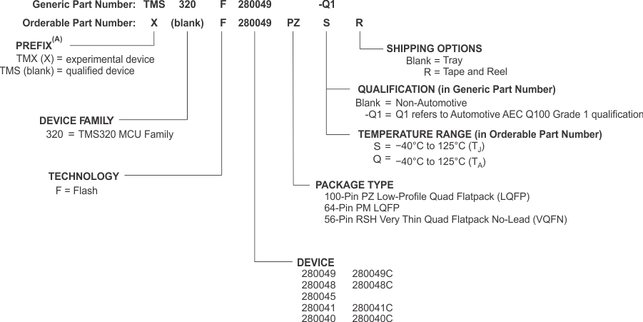
GUID-40DFB575-A0B6-4D73-BBC3-9D00FD9EE88E-low.gif
Prefix X is used in orderable part numbers.
Figure 10-1 Device Nomenclature