SPRS945G January 2017 – January 2023 TMS320F280040-Q1 , TMS320F280040C-Q1 , TMS320F280041 , TMS320F280041-Q1 , TMS320F280041C , TMS320F280041C-Q1 , TMS320F280045 , TMS320F280048-Q1 , TMS320F280048C-Q1 , TMS320F280049 , TMS320F280049-Q1 , TMS320F280049C , TMS320F280049C-Q1
PRODUCTION DATA
- 1 Features
- 2 Applications
- 3 Description
- 4 Revision History
- 5 Device Comparison
- 6 Pin Configuration and Functions
-
7 Specifications
- 7.1 Absolute Maximum Ratings
- 7.2 ESD Ratings – Commercial
- 7.3 ESD Ratings – Automotive
- 7.4 Recommended Operating Conditions
- 7.5 Power Consumption Summary
- 7.6 Electrical Characteristics
- 7.7 Thermal Resistance Characteristics
- 7.8 Thermal Design Considerations
- 7.9
System
- 7.9.1
Power Management Module (PMM)
- 7.9.1.1 Introduction
- 7.9.1.2 Overview
- 7.9.1.3 External Components
- 7.9.1.4 Power Sequencing
- 7.9.1.5 Power Management Module Electrical Data and Timing
- 7.9.2 Reset Timing
- 7.9.3
Clock Specifications
- 7.9.3.1 Clock Sources
- 7.9.3.2 Clock Frequencies, Requirements, and Characteristics
- 7.9.3.3 Input Clocks and PLLs
- 7.9.3.4 Crystal (XTAL) Oscillator
- 7.9.3.5 Internal Oscillators
- 7.9.4 Flash Parameters
- 7.9.5 Emulation/JTAG
- 7.9.6 GPIO Electrical Data and Timing
- 7.9.7 Interrupts
- 7.9.8 Low-Power Modes
- 7.9.1
Power Management Module (PMM)
- 7.10 Analog Peripherals
- 7.11
Control Peripherals
- 7.11.1 Enhanced Capture (eCAP)
- 7.11.2 High-Resolution Capture Submodule (HRCAP6–HRCAP7)
- 7.11.3 Enhanced Pulse Width Modulator (ePWM)
- 7.11.4 High-Resolution Pulse Width Modulator (HRPWM)
- 7.11.5 Enhanced Quadrature Encoder Pulse (eQEP)
- 7.11.6 Sigma-Delta Filter Module (SDFM)
- 7.12
Communications Peripherals
- 7.12.1 Controller Area Network (CAN)
- 7.12.2 Inter-Integrated Circuit (I2C)
- 7.12.3 Power Management Bus (PMBus) Interface
- 7.12.4 Serial Communications Interface (SCI)
- 7.12.5 Serial Peripheral Interface (SPI)
- 7.12.6 Local Interconnect Network (LIN)
- 7.12.7 Fast Serial Interface (FSI)
-
8 Detailed Description
- 8.1 Overview
- 8.2 Functional Block Diagram
- 8.3 Memory
- 8.4 Identification
- 8.5 Bus Architecture – Peripheral Connectivity
- 8.6 C28x Processor
- 8.7 Control Law Accelerator (CLA)
- 8.8 Direct Memory Access (DMA)
- 8.9 Boot ROM and Peripheral Booting
- 8.10 Dual Code Security Module
- 8.11 Watchdog
- 8.12 Configurable Logic Block (CLB)
- 8.13 Functional Safety
- 9 Applications, Implementation, and Layout
- 10Device and Documentation Support
- 11Mechanical, Packaging, and Orderable Information
Package Options
Mechanical Data (Package|Pins)
- PM|64
Thermal pad, mechanical data (Package|Pins)
Orderable Information
7.10.5.1.1 Comparator Electrical Characteristics
| PARAMETER | TEST CONDITIONS | MIN | TYP | MAX | UNIT | |
|---|---|---|---|---|---|---|
| TPU | Power-up time | 500 | µs | |||
| Comparator input (CMPINxx) range | 0 | VDDA | V | |||
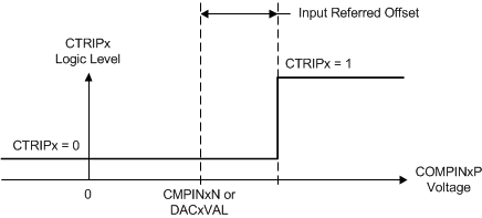
| Input referred offset error | Low common mode, inverting input set to 50 mV | –20 | 20 | mV | ||
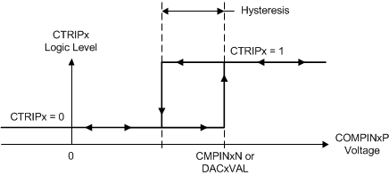
| Hysteresis(1) | 1x | 12 | LSB | |||
| 2x | 24 | |||||
| 3x | 36 | |||||
| 4x | 48 | |||||
| Response time (delay from CMPINx input change to output on ePWM X-BAR or Output X-BAR) | Step response | 21 | 60 | ns | ||
| Ramp response (1.65 V/µs) | 26 | |||||
| Ramp response (8.25 mV/µs) | 30 | ns | ||||
| PSRR | Power Supply Rejection Ratio | Up to 250 kHz | 46 | dB | ||
| CMRR | Common Mode Rejection Ratio | 40 | dB | |||
The CMPSS inputs must be kept below VDDA + 0.3 V to ensure proper functional operation. If a CMPSS input exceeds this level, an internal blocking circuit isolates the internal comparator from the external pin until the external pin voltage returns below VDDA + 0.3 V. During this time, the internal comparator input is floating and can decay below VDDA within approximately 0.5 µs. After this time, the comparator could begin to output an incorrect result depending on the value of the other comparator input.
 Figure 7-58 CMPSS
Comparator Input Referred Offset
 Figure 7-59 CMPSS
Comparator Hysteresis
Figure 7-59 CMPSS
Comparator HysteresisSection 7.10.5.1.2 lists the CMPSS DAC static electrical characteristics.