SPRS945G January 2017 – January 2023 TMS320F280040-Q1 , TMS320F280040C-Q1 , TMS320F280041 , TMS320F280041-Q1 , TMS320F280041C , TMS320F280041C-Q1 , TMS320F280045 , TMS320F280048-Q1 , TMS320F280048C-Q1 , TMS320F280049 , TMS320F280049-Q1 , TMS320F280049C , TMS320F280049C-Q1
PRODUCTION DATA
- 1 Features
- 2 Applications
- 3 Description
- 4 Revision History
- 5 Device Comparison
- 6 Pin Configuration and Functions
-
7 Specifications
- 7.1 Absolute Maximum Ratings
- 7.2 ESD Ratings – Commercial
- 7.3 ESD Ratings – Automotive
- 7.4 Recommended Operating Conditions
- 7.5 Power Consumption Summary
- 7.6 Electrical Characteristics
- 7.7 Thermal Resistance Characteristics
- 7.8 Thermal Design Considerations
- 7.9
System
- 7.9.1
Power Management Module (PMM)
- 7.9.1.1 Introduction
- 7.9.1.2 Overview
- 7.9.1.3 External Components
- 7.9.1.4 Power Sequencing
- 7.9.1.5 Power Management Module Electrical Data and Timing
- 7.9.2 Reset Timing
- 7.9.3
Clock Specifications
- 7.9.3.1 Clock Sources
- 7.9.3.2 Clock Frequencies, Requirements, and Characteristics
- 7.9.3.3 Input Clocks and PLLs
- 7.9.3.4 Crystal (XTAL) Oscillator
- 7.9.3.5 Internal Oscillators
- 7.9.4 Flash Parameters
- 7.9.5 Emulation/JTAG
- 7.9.6 GPIO Electrical Data and Timing
- 7.9.7 Interrupts
- 7.9.8 Low-Power Modes
- 7.9.1
Power Management Module (PMM)
- 7.10 Analog Peripherals
- 7.11
Control Peripherals
- 7.11.1 Enhanced Capture (eCAP)
- 7.11.2 High-Resolution Capture Submodule (HRCAP6–HRCAP7)
- 7.11.3 Enhanced Pulse Width Modulator (ePWM)
- 7.11.4 High-Resolution Pulse Width Modulator (HRPWM)
- 7.11.5 Enhanced Quadrature Encoder Pulse (eQEP)
- 7.11.6 Sigma-Delta Filter Module (SDFM)
- 7.12
Communications Peripherals
- 7.12.1 Controller Area Network (CAN)
- 7.12.2 Inter-Integrated Circuit (I2C)
- 7.12.3 Power Management Bus (PMBus) Interface
- 7.12.4 Serial Communications Interface (SCI)
- 7.12.5 Serial Peripheral Interface (SPI)
- 7.12.6 Local Interconnect Network (LIN)
- 7.12.7 Fast Serial Interface (FSI)
-
8 Detailed Description
- 8.1 Overview
- 8.2 Functional Block Diagram
- 8.3 Memory
- 8.4 Identification
- 8.5 Bus Architecture – Peripheral Connectivity
- 8.6 C28x Processor
- 8.7 Control Law Accelerator (CLA)
- 8.8 Direct Memory Access (DMA)
- 8.9 Boot ROM and Peripheral Booting
- 8.10 Dual Code Security Module
- 8.11 Watchdog
- 8.12 Configurable Logic Block (CLB)
- 8.13 Functional Safety
- 9 Applications, Implementation, and Layout
- 10Device and Documentation Support
- 11Mechanical, Packaging, and Orderable Information
Package Options
Mechanical Data (Package|Pins)
- PM|64
Thermal pad, mechanical data (Package|Pins)
Orderable Information
7.9.5 Emulation/JTAG
The JTAG (IEEE Standard 1149.1-1990 Standard Test Access Port and Boundary Scan Architecture) port has four dedicated pins: TMS, TDI, TDO, and TCK. The cJTAG (IEEE Standard 1149.7-2009 for Reduced-Pin and Enhanced-Functionality Test Access Port and Boundary-Scan Architecture) port is a compact JTAG interface requiring only two pins (TMS and TCK), which allows other device functionality to be muxed to the traditional GPIO35 (TDI) and GPIO37 (TDO) pins.
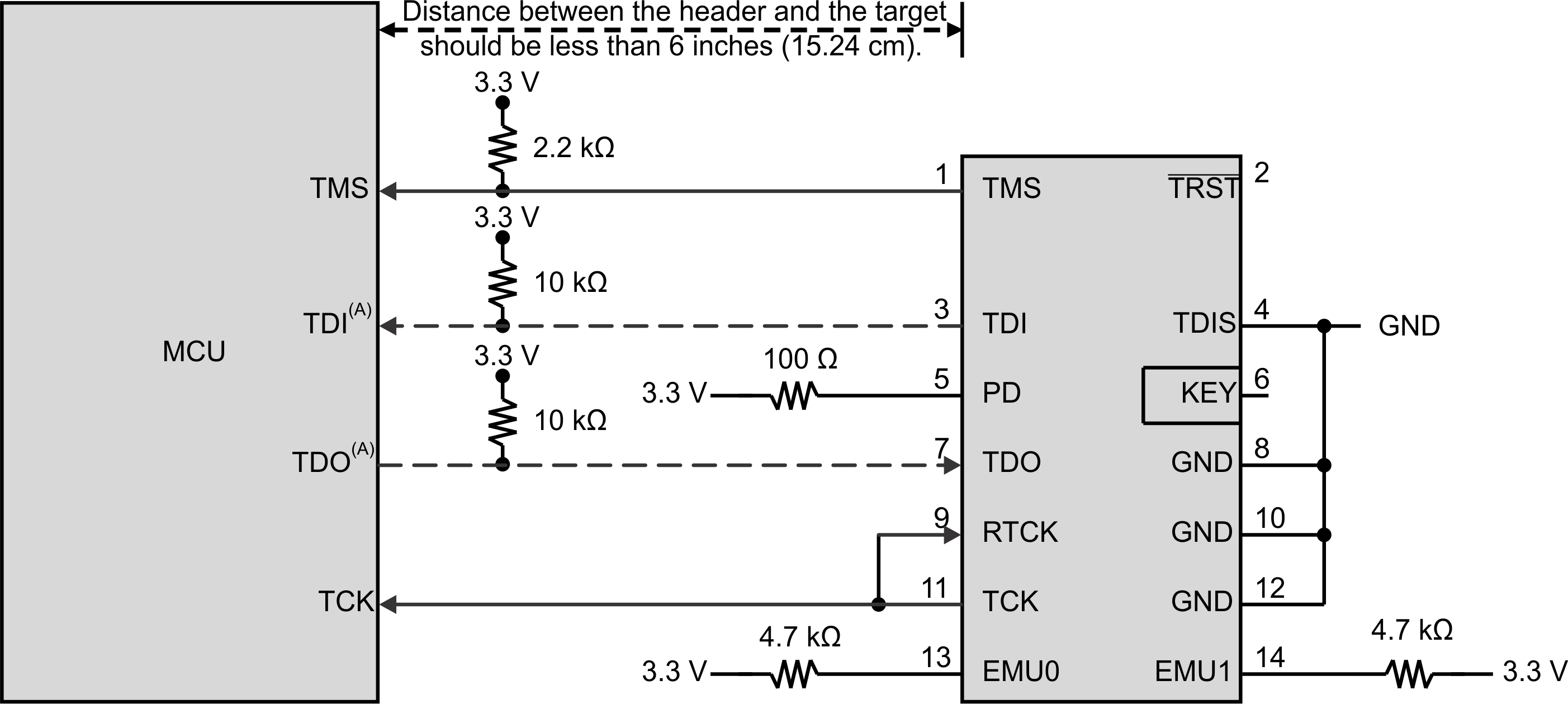
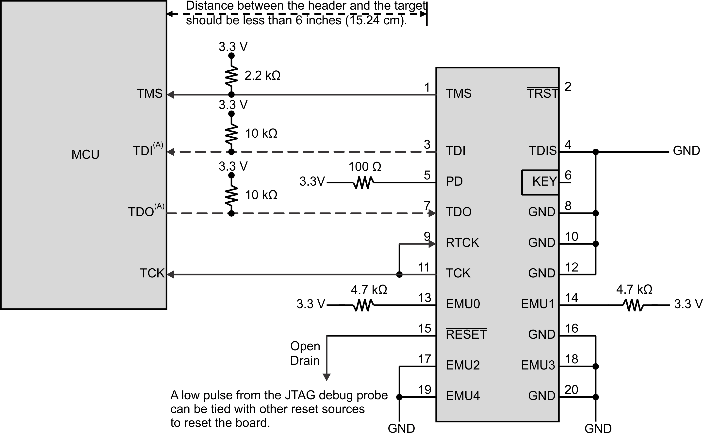
Typically, no buffers are needed on the JTAG signals when the distance between the MCU target and the JTAG header is smaller than 6 inches (15.24 cm), and no other devices are present on the JTAG chain. Otherwise, each signal should be buffered. Additionally, for most JTAG debug probe operations at 10 MHz, no series resistors are needed on the JTAG signals. However, if high emulation speeds are expected (35 MHz or so), 22-Ω resistors should be placed in series on each JTAG signal.
The PD (Power Detect) terminal of the JTAG debug probe header should be connected to the board's 3.3-V supply. Header GND terminals should be connected to board ground. TDIS (Cable Disconnect Sense) should also be connected to board ground. The JTAG clock should be looped from the header TCK output terminal back to the RTCK input terminal of the header (to sense clock continuity by the JTAG debug probe). This MCU does not support the EMU0 and EMU1 signals that are present on 14-pin and 20-pin emulation headers. These signals should always be pulled up at the emulation header through a pair of board pullup resistors ranging from 2.2 kΩ to 4.7 kΩ (depending on the drive strength of the debugger ports). Typically, a 2.2-kΩ value is used.
Header terminal RESET is an open-drain output from the JTAG debug probe header that enables board components to be reset through JTAG debug probe commands (available only through the 20-pin header). Figure 7-26 shows how the 14-pin JTAG header connects to the MCU’s JTAG port signals. Figure 7-27 shows how to connect to the 20-pin JTAG header. The 20-pin JTAG header terminals EMU2, EMU3, and EMU4 are not used and should be grounded.
For more information about hardware breakpoints and watchpoints, see Hardware Breakpoints and Watchpoints for C28x in CCS.
For more information about JTAG emulation, see the XDS Target Connection Guide.
JTAG Test Data Input (TDI) is the default mux selection for the pin. The internal pullup is disabled by default. If this pin is used as JTAG TDI, the internal pullup should be enabled or an external pullup added on the board to avoid a floating input. In the cJTAG option, this pin can be used as GPIO.
JTAG Test Data Output (TDO) is the default mux selection for the pin. The internal pullup is disabled by default. The TDO function will be in a tri-state condition when there is no JTAG activity, leaving this pin floating. The internal pullup should be enabled or an external pullup added on the board to avoid a floating GPIO input. In the cJTAG option, this pin can be used as GPIO.

