SPRSP25A June   2018  – July 2018 TMS320F28035-EP

PRODUCTION DATA.  

  1. 1Device Overview
    1. 1.1 Features
    2. 1.2 Applications
    3. 1.3 Description
    4. 1.4 Functional Block Diagram
  2. 2Revision History
  3. 3Terminal Configuration and Functions
    1. 3.1 Pin Diagram
    2. 3.2 Signal Descriptions
      1. Table 3-1 Signal Descriptions
  4. 4Specifications
    1. 4.1  Absolute Maximum Ratings
    2. 4.2  ESD Ratings
    3. 4.3  Power-On Hours (POH) Limits
    4. 4.4  Recommended Operating Conditions
    5. 4.5  Power Consumption Summary
      1. Table 4-1 TMS320F2803x Current Consumption at 60-MHz SYSCLKOUT
      2. 4.5.1      Reducing Current Consumption
      3. 4.5.2      Current Consumption Graphs (VREG Enabled)
    6. 4.6  Electrical Characteristics
    7. 4.7  Thermal Resistance Characteristics
    8. 4.8  Thermal Design Considerations
    9. 4.9  Emulator Connection Without Signal Buffering for the MCU
    10. 4.10 Parameter Information
      1. 4.10.1 Timing Parameter Symbology
      2. 4.10.2 General Notes on Timing Parameters
    11. 4.11 Test Load Circuit
    12. 4.12 Power Sequencing
      1. Table 4-4 Reset (XRS) Timing Requirements
      2. Table 4-5 Reset (XRS) Switching Characteristics
    13. 4.13 Clock Specifications
      1. 4.13.1 Device Clock Table
        1. Table 4-6 2803x Clock Table and Nomenclature (60-MHz Devices)
        2. Table 4-7 Device Clocking Requirements/Characteristics
        3. Table 4-8 Internal Zero-Pin Oscillator (INTOSC1/INTOSC2) Characteristics
      2. 4.13.2 Clock Requirements and Characteristics
        1. Table 4-9   XCLKIN Timing Requirements – PLL Enabled
        2. Table 4-10 XCLKIN Timing Requirements – PLL Disabled
        3. Table 4-11 XCLKOUT Switching Characteristics (PLL Bypassed or Enabled)
    14. 4.14 Flash Timing
      1. Table 4-12 Flash/OTP Endurance
      2. Table 4-13 Flash Parameters at 60-MHz SYSCLKOUT
      3. Table 4-14 Flash/OTP Access Timing
      4. Table 4-15 Flash Data Retention Duration
  5. 5Detailed Description
    1. 5.1 Overview
      1. 5.1.1  CPU
      2. 5.1.2  Control Law Accelerator (CLA)
      3. 5.1.3  Memory Bus (Harvard Bus Architecture)
      4. 5.1.4  Peripheral Bus
      5. 5.1.5  Real-Time JTAG and Analysis
      6. 5.1.6  Flash
      7. 5.1.7  M0, M1 SARAMs
      8. 5.1.8  L0 SARAM, and L1, L2, and L3 DPSARAMs
      9. 5.1.9  Boot ROM
        1. 5.1.9.1 Emulation Boot
        2. 5.1.9.2 GetMode
        3. 5.1.9.3 Peripheral Pins Used by the Bootloader
      10. 5.1.10 Security
      11. 5.1.11 Peripheral Interrupt Expansion (PIE) Block
      12. 5.1.12 External Interrupts (XINT1–XINT3)
      13. 5.1.13 Internal Zero Pin Oscillators, Oscillator, and PLL
      14. 5.1.14 Watchdog
      15. 5.1.15 Peripheral Clocking
      16. 5.1.16 Low-power Modes
      17. 5.1.17 Peripheral Frames 0, 1, 2, 3 (PFn)
      18. 5.1.18 General-Purpose Input/Output (GPIO) Multiplexer
      19. 5.1.19 32-Bit CPU-Timers (0, 1, 2)
      20. 5.1.20 Control Peripherals
      21. 5.1.21 Serial Port Peripherals
    2. 5.2 Memory Maps
    3. 5.3 Register Maps
    4. 5.4 Device Emulation Registers
    5. 5.5 VREG/BOR/POR
      1. 5.5.1 On-chip Voltage Regulator (VREG)
        1. 5.5.1.1 Using the On-chip VREG
        2. 5.5.1.2 Disabling the On-chip VREG
      2. 5.5.2 On-chip Power-On Reset (POR) and Brown-Out Reset (BOR) Circuit
    6. 5.6 System Control
      1. 5.6.1 Internal Zero Pin Oscillators
      2. 5.6.2 Crystal Oscillator Option
      3. 5.6.3 PLL-Based Clock Module
      4. 5.6.4 Loss of Input Clock (NMI Watchdog Function)
      5. 5.6.5 CPU-Watchdog Module
    7. 5.7 Low-Power Modes Block
    8. 5.8 Interrupts
      1. 5.8.1 External Interrupts
        1. 5.8.1.1 External Interrupt Electrical Data/Timing
          1. Table 5-20 External Interrupt Timing Requirements
          2. Table 5-21 External Interrupt Switching Characteristics
    9. 5.9 Peripherals
      1. 5.9.1  Control Law Accelerator (CLA) Overview
      2. 5.9.2  Analog Block
        1. 5.9.2.1 Analog-to-Digital Converter (ADC)
          1. 5.9.2.1.1 Features
          2. 5.9.2.1.2 ADC Start-of-Conversion Electrical Data/Timing
            1. Table 5-26 External ADC Start-of-Conversion Switching Characteristics
          3. 5.9.2.1.3 On-Chip Analog-to-Digital Converter (ADC) Electrical Data/Timing
            1. Table 5-27 ADC Electrical Characteristics
            2. Table 5-28 ADC Power Modes
            3. 5.9.2.1.3.1 Internal Temperature Sensor
              1. Table 5-29 Temperature Sensor Coefficient
            4. 5.9.2.1.3.2 ADC Power-Up Control Bit Timing
              1. Table 5-30 ADC Power-Up Delays
            5. 5.9.2.1.3.3 ADC Sequential and Simultaneous Timings
        2. 5.9.2.2 ADC MUX
        3. 5.9.2.3 Comparator Block
          1. 5.9.2.3.1 On-Chip Comparator/DAC Electrical Data/Timing
            1. Table 5-32 Electrical Characteristics of the Comparator/DAC
      3. 5.9.3  Detailed Descriptions
      4. 5.9.4  Serial Peripheral Interface (SPI) Module
        1. 5.9.4.1 SPI Master Mode Electrical Data/Timing
          1. Table 5-35 SPI Master Mode External Timing (Clock Phase = 0)
          2. Table 5-36 SPI Master Mode External Timing (Clock Phase = 1)
        2. 5.9.4.2 SPI Slave Mode Electrical Data/Timing
          1. Table 5-37 SPI Slave Mode External Timing (Clock Phase = 0)
          2. Table 5-38 SPI Slave Mode External Timing (Clock Phase = 1)
      5. 5.9.5  Serial Communications Interface (SCI) Module
      6. 5.9.6  Local Interconnect Network (LIN)
      7. 5.9.7  Enhanced Controller Area Network (eCAN) Module
      8. 5.9.8  Inter-Integrated Circuit (I2C)
        1. 5.9.8.1 I2C Electrical Data/Timing
          1. Table 5-44 I2C Timing Requirements
          2. Table 5-45 I2C Switching Characteristics
      9. 5.9.9  Enhanced PWM Modules (ePWM1/2/3/4/5/6/7)
        1. 5.9.9.1 ePWM Electrical Data/Timing
          1. Table 5-48 ePWM Timing Requirements
          2. Table 5-49 ePWM Switching Characteristics
        2. 5.9.9.2 Trip-Zone Input Timing
          1. Table 5-50 Trip-Zone Input Timing Requirements
      10. 5.9.10 High-Resolution PWM (HRPWM)
        1. 5.9.10.1 HRPWM Electrical Data/Timing
          1. Table 5-51 High-Resolution PWM Characteristics
      11. 5.9.11 Enhanced Capture Module (eCAP1)
        1. 5.9.11.1 eCAP Electrical Data/Timing
          1. Table 5-53 Enhanced Capture (eCAP) Timing Requirement
          2. Table 5-54 eCAP Switching Characteristics
      12. 5.9.12 High-Resolution Capture (HRCAP) Module
        1. 5.9.12.1 HRCAP Electrical Data/Timing
          1. Table 5-56 High-Resolution Capture (HRCAP) Timing Requirements
      13. 5.9.13 Enhanced Quadrature Encoder Pulse (eQEP)
        1. 5.9.13.1 eQEP Electrical Data/Timing
          1. Table 5-58 Enhanced Quadrature Encoder Pulse (eQEP) Timing Requirements
          2. Table 5-59 eQEP Switching Characteristics
      14. 5.9.14 JTAG Port
      15. 5.9.15 General-Purpose Input/Output (GPIO) MUX
        1. 5.9.15.1 GPIO Electrical Data/Timing
          1. 5.9.15.1.1 GPIO - Output Timing
            1. Table 5-63 General-Purpose Output Switching Characteristics
          2. 5.9.15.1.2 GPIO - Input Timing
            1. Table 5-64 General-Purpose Input Timing Requirements
          3. 5.9.15.1.3 Sampling Window Width for Input Signals
          4. 5.9.15.1.4 Low-Power Mode Wakeup Timing
            1. Table 5-65 IDLE Mode Timing Requirements
            2. Table 5-66 IDLE Mode Switching Characteristics
            3. Table 5-67 STANDBY Mode Timing Requirements
            4. Table 5-68 STANDBY Mode Switching Characteristics
            5. Table 5-69 HALT Mode Timing Requirements
            6. Table 5-70 HALT Mode Switching Characteristics
  6. 6Applications, Implementation, and Layout
    1. 6.1 TI Design or Reference Design
  7. 7Device and Documentation Support
    1. 7.1 Getting Started
    2. 7.2 Device and Development Support Tool Nomenclature
    3. 7.3 Tools and Software
    4. 7.4 Documentation Support
    5. 7.5 Community Resources
    6. 7.6 Trademarks
    7. 7.7 Electrostatic Discharge Caution
    8. 7.8 Glossary
  8. 8Mechanical, Packaging, and Orderable Information
    1. 8.1 Packaging Information

Package Options

Mechanical Data (Package|Pins)
Thermal pad, mechanical data (Package|Pins)
Orderable Information

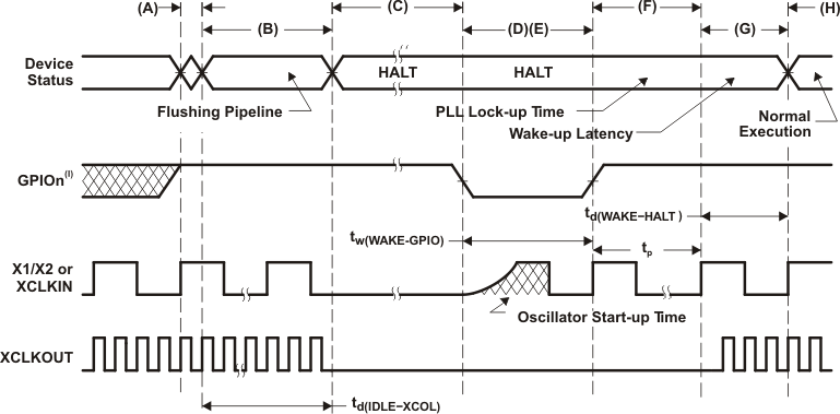
Table 5-70 HALT Mode Switching Characteristics

over recommended operating conditions (unless otherwise noted)
PARAMETER MIN MAX UNIT
td(IDLE-XCOL) Delay time, IDLE instruction executed to XCLKOUT low 32tc(SCO) 45tc(SCO) cycles
tp PLL lock-up time 1 ms
td(WAKE-HALT) Delay time, PLL lock to program execution resume
  • Wake up from flash
    • Flash module in sleep state
1125tc(SCO) cycles
  • Wake up from SARAM
35tc(SCO) cycles
TMS320F28035-EP td_halt_wk_prs584.gif
IDLE instruction is executed to put the device into HALT mode.
The PLL block responds to the HALT signal. SYSCLKOUT is held for the number of cycles indicated below before oscillator is turned off and the CLKIN to the core is stopped:
  • 16 cycles, when DIVSEL = 00 or 01
  • 32 cycles, when DIVSEL = 10
  • 64 cycles, when DIVSEL = 11
This delay enables the CPU pipeline and any other pending operations to flush properly.
Clocks to the peripherals are turned off and the PLL is shut down. If a quartz crystal or ceramic resonator is used as the clock source, the internal oscillator is shut down as well. The device is now in HALT mode and consumes absolute minimum power. It is possible to keep the zero-pin internal oscillators (INTOSC1 and INTOSC2) and the watchdog alive in HALT mode. This is done by writing to the appropriate bits in the CLKCTL register. After the IDLE instruction is executed, a delay of 5 OSCCLK cycles (minimum) is needed before the wake-up signal could be asserted.
When the GPIOn pin (used to bring the device out of HALT) is driven low, the oscillator is turned on and the oscillator wake-up sequence is initiated. The GPIO pin should be driven high only after the oscillator has stabilized. This enables the provision of a clean clock signal during the PLL lock sequence. Because the falling edge of the GPIO pin asynchronously begins the wake-up procedure, care should be taken to maintain a low noise environment prior to entering and during HALT mode.
The wake-up signal fed to a GPIO pin to wake up the device must meet the minimum pulse width requirement. Furthermore, this signal must be free of glitches. If a noisy signal is fed to a GPIO pin, the wake-up behavior of the device will not be deterministic and the device may not exit low-power mode for subsequent wake-up pulses.
Once the oscillator has stabilized, the PLL lock sequence is initiated, which takes 1 ms.
When CLKIN to the core is enabled, the device will respond to the interrupt (if enabled), after a latency. The HALT mode is now exited.
Normal operation resumes.
From the time the IDLE instruction is executed to place the device into low-power mode (LPM), wakeup should not be initiated until at least 4 OSCCLK cycles have elapsed.
Figure 5-49 HALT Mode Wakeup Using GPIOn