SPRS357D August   2006  – June 2020 TMS320F28044

PRODUCTION DATA.  

  1. 1Device Overview
    1. 1.1 Features
    2. 1.2 Applications
    3. 1.3 Description
    4. 1.4 Functional Block Diagram
  2. 2Revision History
  3. 3Device Comparison
    1. 3.1 Related Products
  4. 4Terminal Configuration and Functions
    1. 4.1 Pin Diagrams
    2. 4.2 Signal Descriptions
  5. 5Specifications
    1. 5.1  Absolute Maximum Ratings
    2. 5.2  ESD Ratings – Commercial
    3. 5.3  Recommended Operating Conditions
    4. 5.4  Power Consumption Summary
      1. Table 5-1 TMS320F28044 Current Consumption by Power-Supply Pins at 100-MHz SYSCLKOUT
      2. 5.4.1     Reducing Current Consumption
    5. 5.5  Electrical Characteristics
    6. 5.6  Thermal Resistance Characteristics for F28044 100-Ball GGM Package
    7. 5.7  Thermal Resistance Characteristics for F28044 100-Pin PZ Package
    8. 5.8  Thermal Design Considerations
    9. 5.9  Timing and Switching Characteristics
      1. 5.9.1 Timing Parameter Symbology
        1. 5.9.1.1 General Notes on Timing Parameters
        2. 5.9.1.2 Test Load Circuit
        3. 5.9.1.3 Device Clock Table
          1. Table 5-3 TMS320x280x Clock Table and Nomenclature
      2. 5.9.2 Power Sequencing
        1. 5.9.2.1   Power Management and Supervisory Circuit Solutions
        2. Table 5-5 Reset (XRS) Timing Requirements
      3. 5.9.3 Clock Requirements and Characteristics
        1. Table 5-6 Input Clock Frequency
        2. Table 5-7 XCLKIN Timing Requirements - PLL Enabled
        3. Table 5-8 XCLKIN Timing Requirements - PLL Disabled
        4. Table 5-9 XCLKOUT Switching Characteristics (PLL Bypassed or Enabled)
      4. 5.9.4 Peripherals
        1. 5.9.4.1 General-Purpose Input/Output (GPIO)
          1. 5.9.4.1.1 GPIO - Output Timing
            1. Table 5-10 General-Purpose Output Switching Characteristics
          2. 5.9.4.1.2 GPIO - Input Timing
            1. Table 5-11 General-Purpose Input Timing Requirements
          3. 5.9.4.1.3 Sampling Window Width for Input Signals
          4. 5.9.4.1.4 Low-Power Mode Wakeup Timing
            1. Table 5-12 IDLE Mode Timing Requirements
            2. Table 5-13 IDLE Mode Switching Characteristics
            3. Table 5-14 STANDBY Mode Timing Requirements
            4. Table 5-15 STANDBY Mode Switching Characteristics
            5. Table 5-16 HALT Mode Timing Requirements
            6. Table 5-17 HALT Mode Switching Characteristics
        2. 5.9.4.2 Enhanced Control Peripherals
          1. 5.9.4.2.1 Enhanced Pulse Width Modulator (ePWM) Timing
            1. Table 5-18 ePWM Timing Requirements
            2. Table 5-19 ePWM Switching Characteristics
          2. 5.9.4.2.2 Trip-Zone Input Timing
            1. Table 5-20 Trip-Zone input Timing Requirements
          3. 5.9.4.2.3 High-Resolution PWM Timing
            1. Table 5-21 High Resolution PWM Characteristics at SYSCLKOUT = (60 - 100 MHz)
          4. 5.9.4.2.4 ADC Start-of-Conversion Timing
            1. Table 5-22 External ADC Start-of-Conversion Switching Characteristics
        3. 5.9.4.3 External Interrupt Timing
          1. Table 5-23 External Interrupt Timing Requirements
          2. Table 5-24 External Interrupt Switching Characteristics
        4. 5.9.4.4 I2C Electrical Specification and Timing
          1. Table 5-25 I2C Timing
        5. 5.9.4.5 Serial Peripheral Interface (SPI) Master Mode Timing
          1. Table 5-26 SPI Master Mode External Timing (Clock Phase = 0)
          2. Table 5-27 SPI Master Mode External Timing (Clock Phase = 1)
        6. 5.9.4.6 SPI Slave Mode Timing
          1. Table 5-28 SPI Slave Mode External Timing (Clock Phase = 0)
          2. Table 5-29 SPI Slave Mode External Timing (Clock Phase = 1)
      5. 5.9.5 JTAG Debug Probe Connection Without Signal Buffering for the DSP
      6. 5.9.6 Flash Timing
        1. Table 5-30 Flash Endurance for A Temperature Material
        2. Table 5-31 Flash Parameters at 100-MHz SYSCLKOUT
        3. Table 5-32 Flash/OTP Access Timing
        4. Table 5-33 Flash Data Retention Duration
    10. 5.10 On-Chip Analog-to-Digital Converter
      1. Table 5-35 ADC Electrical Characteristics (over recommended operating conditions)
      2. 5.10.1     ADC Power-Up Control Bit Timing
        1. Table 5-36 ADC Power-Up Delays
        2. Table 5-37 Current Consumption for Different ADC Configurations (at 25-MHz ADCCLK)
      3. 5.10.2     Definitions
      4. 5.10.3     Sequential Sampling Mode (Single-Channel) (SMODE = 0)
        1. Table 5-38 Sequential Sampling Mode Timing
      5. 5.10.4     Simultaneous Sampling Mode (Dual-Channel) (SMODE = 1)
        1. Table 5-39 Simultaneous Sampling Mode Timing
      6. 5.10.5     Detailed Descriptions
  6. 6Detailed Description
    1. 6.1 Brief Descriptions
      1. 6.1.1  C28x CPU
      2. 6.1.2  Memory Bus (Harvard Bus Architecture)
      3. 6.1.3  Peripheral Bus
      4. 6.1.4  Real-Time JTAG and Analysis
      5. 6.1.5  Flash
      6. 6.1.6  M0, M1 SARAMs
      7. 6.1.7  L0, L1 SARAMs
      8. 6.1.8  Boot ROM
      9. 6.1.9  Security
      10. 6.1.10 Peripheral Interrupt Expansion (PIE) Block
      11. 6.1.11 External Interrupts (XINT1, XINT2, XNMI)
      12. 6.1.12 Oscillator and PLL
      13. 6.1.13 Watchdog
      14. 6.1.14 Peripheral Clocking
      15. 6.1.15 Low-Power Modes
      16. 6.1.16 Peripheral Frames 0, 1, 2 (PFn)
      17. 6.1.17 General-Purpose Input/Output (GPIO) Multiplexer
      18. 6.1.18 32-Bit CPU-Timers (0, 1, 2)
      19. 6.1.19 Control Peripherals
      20. 6.1.20 Serial Port Peripherals
    2. 6.2 Peripherals
      1. 6.2.1 32-Bit CPU-Timers 0/1/2
      2. 6.2.2 Enhanced PWM Modules (ePWM1–16)
      3. 6.2.3 Hi-Resolution PWM (HRPWM)
      4. 6.2.4 Enhanced Analog-to-Digital Converter (ADC) Module
        1. 6.2.4.1 ADC Connections if the ADC Is Not Used
        2. 6.2.4.2 ADC Registers
      5. 6.2.5 Serial Communications Interface (SCI) Module (SCI-A)
      6. 6.2.6 Serial Peripheral Interface (SPI) Module (SPI-A)
      7. 6.2.7 Inter-Integrated Circuit (I2C)
      8. 6.2.8 GPIO MUX
    3. 6.3 Memory Map
    4. 6.4 Register Map
      1. 6.4.1 Device Emulation Registers
    5. 6.5 Interrupts
      1. 6.5.1 External Interrupts
    6. 6.6 System Control
      1. 6.6.1 OSC and PLL Block
        1. 6.6.1.1 External Reference Oscillator Clock Option
        2. 6.6.1.2 PLL-Based Clock Module
        3. 6.6.1.3 Loss of Input Clock
      2. 6.6.2 Watchdog Block
    7. 6.7 Low-Power Modes Block
  7. 7Applications, Implementation, and Layout
    1. 7.1 TI Reference Design
  8. 8Device and Documentation Support
    1. 8.1 Getting Started
    2. 8.2 Device and Development Support Tool Nomenclature
    3. 8.3 Tools and Software
    4. 8.4 Documentation Support
    5. 8.5 Support Resources
    6. 8.6 Trademarks
    7. 8.7 Electrostatic Discharge Caution
    8. 8.8 Glossary
  9. 9Mechanical, Packaging, and Orderable Information
    1. 9.1 Packaging Information

Package Options

Refer to the PDF data sheet for device specific package drawings

Mechanical Data (Package|Pins)
  • PZ|100
Thermal pad, mechanical data (Package|Pins)
Orderable Information

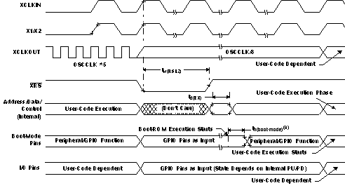
Table 5-5 Reset (XRS) Timing Requirements

MIN NOM MAX UNIT
tw(RSL1)(1) Pulse duration, stable XCLKIN to XRS high 8tc(OSCCLK) cycles
tw(RSL2) Pulse duration, XRS low Warm reset 8tc(OSCCLK) cycles
tw(WDRS) Pulse duration, reset pulse generated by watchdog 512tc(OSCCLK) cycles
td(EX) Delay time, address/data valid after XRS high 32tc(OSCCLK) cycles
tOSCST(2) Oscillator start-up time 1 10 ms
th(boot-mode) Hold time for boot-mode pins 200tc(OSCCLK) cycles
In addition to the tw(RSL1) requirement, XRS has to be low at least for 1 ms after VDD reaches 1.5 V.
Dependent on crystal/resonator and board design.
TMS320F28044 td_wmres_prs357.gif
After reset, the Boot ROM code samples BOOT Mode pins. Based on the status of the Boot Mode pin, the boot code branches to destination memory or boot code function. If Boot ROM code executes after power-on conditions (in debugger environment), the Boot code execution time is based on the current SYSCLKOUT speed. The SYSCLKOUT will be based on user environment and could be with or without PLL enabled.
Figure 5-3 Warm Reset

Figure 5-4 shows an example for the effect of writing into PLLCR register. In the first phase, PLLCR = 0x0004 and SYSCLKOUT = OSCCLK x 2. The PLLCR is then written with 0x0008. Right after the PLLCR register is written, the PLL lock-up phase begins. During this phase, SYSCLKOUT = OSCCLK/2. After the PLL lock-up is complete (which takes 131072 OSCCLK cycles), SYSCLKOUT reflects the new operating frequency, OSCCLK x 4.

TMS320F28044 td_pllcrw_prs357.gifFigure 5-4 Example of Effect of Writing Into PLLCR Register