SPRS902K October 2014 – February 2024 TMS320F28075 , TMS320F28075-Q1 , TMS320F28076
PRODUCTION DATA
- 1
- 1 Features
- 2 Applications
- 3 Description
- 4 Device Comparison
- 5 Pin Configuration and Functions
-
6 Specifications
- 6.1 Absolute Maximum Ratings
- 6.2 ESD Ratings – Commercial
- 6.3 ESD Ratings – Automotive
- 6.4 Recommended Operating Conditions
- 6.5 Power Consumption Summary
- 6.6 Electrical Characteristics
- 6.7 Thermal Resistance Characteristics
- 6.8 Thermal Design Considerations
- 6.9
System
- 6.9.1 Power Management
- 6.9.2 Reset Timing
- 6.9.3
Clock Specifications
- 6.9.3.1 Clock Sources
- 6.9.3.2 Clock Frequencies, Requirements, and Characteristics
- 6.9.3.3 Input Clocks and PLLs
- 6.9.3.4 XTAL Oscillator
- 6.9.3.5 Internal Oscillators
- 6.9.4 Flash Parameters
- 6.9.5 RAM Specifications
- 6.9.6 ROM Specifications
- 6.9.7 Emulation/JTAG
- 6.9.8 GPIO Electrical Data and Timing
- 6.9.9 Interrupts
- 6.9.10
Low-Power Modes
- 6.9.10.1 Clock-Gating Low-Power Modes
- 6.9.10.2 Power-Gating Low-Power Modes
- 6.9.10.3
Low-Power Mode Wakeup Timing
- 6.9.10.3.1 IDLE Mode Timing Requirements
- 6.9.10.3.2 IDLE Mode Switching Characteristics
- 6.9.10.3.3 STANDBY Mode Timing Requirements
- 6.9.10.3.4 STANDBY Mode Switching Characteristics
- 6.9.10.3.5 HALT Mode Timing Requirements
- 6.9.10.3.6 HALT Mode Switching Characteristics
- 6.9.10.3.7 HIBERNATE Mode Timing Requirements
- 6.9.10.3.8 HIBERNATE Mode Switching Characteristics
- 6.9.11 External Memory Interface (EMIF)
- 6.10 Analog Peripherals
- 6.11
Control Peripherals
- 6.11.1 Enhanced Capture (eCAP)
- 6.11.2 Enhanced Pulse Width Modulator (ePWM)
- 6.11.3 Enhanced Quadrature Encoder Pulse (eQEP)
- 6.11.4 High-Resolution Pulse Width Modulator (HRPWM)
- 6.11.5 Sigma-Delta Filter Module (SDFM)
- 6.12
Communications Peripherals
- 6.12.1 Controller Area Network (CAN)
- 6.12.2 Inter-Integrated Circuit (I2C)
- 6.12.3 Multichannel Buffered Serial Port (McBSP)
- 6.12.4 Serial Communications Interface (SCI)
- 6.12.5 Serial Peripheral Interface (SPI)
- 6.12.6 Universal Serial Bus (USB) Controller
-
7 Detailed Description
- 7.1 Overview
- 7.2 Functional Block Diagram
- 7.3 Memory
- 7.4 Identification
- 7.5 Bus Architecture – Peripheral Connectivity
- 7.6 C28x Processor
- 7.7 Control Law Accelerator
- 7.8 Direct Memory Access
- 7.9 Boot ROM and Peripheral Booting
- 7.10 Dual Code Security Module
- 7.11 Timers
- 7.12 Nonmaskable Interrupt With Watchdog Timer (NMIWD)
- 7.13 Watchdog
- 7.14 Configurable Logic Block (CLB)
- 7.15 Functional Safety
-
8 Applications, Implementation, and Layout
- 8.1 Application and Implementation
- 8.2 Key Device Features
- 8.3 Application Information
- 9 Device and Documentation Support
- 10Revision History
- 11Mechanical, Packaging, and Orderable Information
Package Options
Refer to the PDF data sheet for device specific package drawings
Mechanical Data (Package|Pins)
- PZP|100
- PTP|176
Thermal pad, mechanical data (Package|Pins)
Orderable Information
6.12.4 Serial Communications Interface (SCI)
The SCI is a 2-wire asynchronous serial port, commonly known as a UART. The SCI module supports digital communications between the CPU and other asynchronous peripherals that use the standard non-return-to-zero (NRZ) format
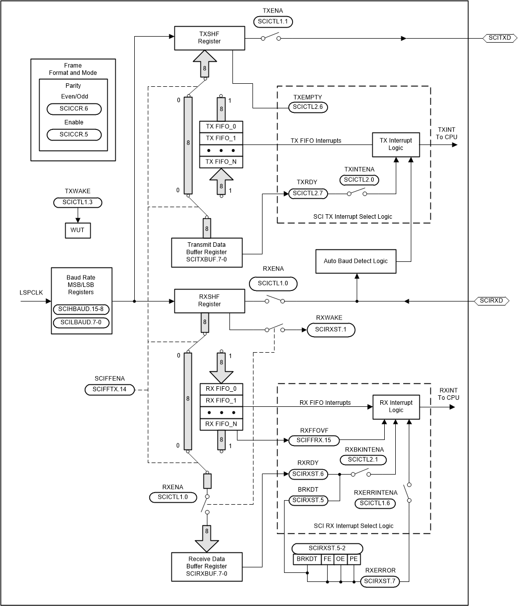
The SCI receiver and transmitter each have a 16-level-deep FIFO for reducing servicing overhead, and each has its own separate enable and interrupt bits. Both can be operated independently for half-duplex communication, or simultaneously for full-duplex communication. To specify data integrity, the SCI checks received data for break detection, parity, overrun, and framing errors. The bit rate is programmable to different speeds through a 16-bit baud-select register. Figure 6-71 shows the SCI block diagram.
Features of the SCI module include:
- Two external pins:
- SCITXD: SCI transmit-output pin
- SCIRXD: SCI receive-input pin
Note: NOTE: Both pins can be used as GPIO if not used for SCI.
- Baud rate programmable to 64K different rates
- Data-word format
- One start bit
- Data-word length programmable from 1 to 8 bits
- Optional even/odd/no parity bit
- 1 or 2 stop bits
- Four error-detection flags: parity, overrun, framing, and break detection
- Two wakeup multiprocessor modes: idle-line and address bit
- Half- or full-duplex operation
- Double-buffered receive and transmit functions
- Transmitter and receiver operations can be accomplished through interrupt-driven or polled algorithms with status flags.
- Transmitter: TXRDY flag (transmitter-buffer register is ready to receive another character) and TX EMPTY flag (transmitter-shift register is empty)
- Receiver: RXRDY flag (receiver-buffer register is ready to receive another character), BRKDT flag (break condition occurred), and RX ERROR flag (monitoring four interrupt conditions)
- Separate enable bits for transmitter and receiver interrupts (except BRKDT)
- NRZ format
- Auto baud-detect hardware logic
- 16-level transmit and receive FIFO
All registers in this module are 8-bit registers. When a register is accessed, the register data is in the lower byte (bits 7–0), and the upper byte (bits 15–8) is read as zeros. Writing to the upper byte has no effect.
 Figure 6-71 SCI Block Diagram
The major elements used in full-duplex operation include:
- A transmitter (TX) and its major registers:
- SCITXBUF register – Transmitter Data Buffer register. Contains data (loaded by the CPU) to be transmitted
- TXSHF register – Transmitter Shift register. Accepts data from the SCITXBUF register and shifts data onto the SCITXD pin, 1 bit at a time
- A receiver (RX) and its major registers:
- RXSHF register – Receiver Shift register. Shifts data in from the SCIRXD pin, 1 bit at a time
- SCIRXBUF register – Receiver Data Buffer register. Contains data to be read by the CPU. Data from a remote processor is loaded into the RXSHF register and then into the SCIRXBUF and SCIRXEMU registers
- A programmable baud generator
- Data-memory-mapped control and status registers enable the CPU to access the I2C module registers and FIFOs.
The SCI receiver and transmitter operate independently.