SPRS439Q June 2007 – August 2022 TMS320F28232 , TMS320F28232-Q1 , TMS320F28234 , TMS320F28234-Q1 , TMS320F28235 , TMS320F28235-Q1 , TMS320F28332 , TMS320F28333 , TMS320F28334 , TMS320F28335 , TMS320F28335-Q1
PRODUCTION DATA
- 1 Features
- 2 Applications
- 3 Description
- 4 Revision History
- 5 Device Comparison
- 6 Terminal Configuration and Functions
-
7 Specifications
- 7.1 Absolute Maximum Ratings
- 7.2 ESD Ratings – Automotive
- 7.3 ESD Ratings – Commercial
- 7.4 Recommended Operating Conditions
- 7.5 Power Consumption Summary
- 7.6 Electrical Characteristics
- 7.7 Thermal Resistance Characteristics
- 7.8 Thermal Design Considerations
- 7.9
Timing and Switching Characteristics
- 7.9.1 Timing Parameter Symbology
- 7.9.2 Power Sequencing
- 7.9.3 Clock Requirements and Characteristics
- 7.9.4
Peripherals
- 7.9.4.1
General-Purpose Input/Output (GPIO)
- 7.9.4.1.1 GPIO - Output Timing
- 7.9.4.1.2 GPIO - Input Timing
- 7.9.4.1.3 Sampling Window Width for Input Signals
- 7.9.4.1.4
Low-Power Mode Wakeup Timing
- 7.9.4.1.4.1 IDLE Mode Timing Requirements
- 7.9.4.1.4.2 IDLE Mode Switching Characteristics
- 7.9.4.1.4.3 IDLE Mode Timing Diagram
- 7.9.4.1.4.4 STANDBY Mode Timing Requirements
- 7.9.4.1.4.5 STANDBY Mode Switching Characteristics
- 7.9.4.1.4.6 STANDBY Mode Timing Diagram
- 7.9.4.1.4.7 HALT Mode Timing Requirements
- 7.9.4.1.4.8 HALT Mode Switching Characteristics
- 7.9.4.1.4.9 HALT Mode Timing Diagram
- 7.9.4.2 Enhanced Control Peripherals
- 7.9.4.3 External Interrupt Timing
- 7.9.4.4 I2C Electrical Specification and Timing
- 7.9.4.5 Serial Peripheral Interface (SPI) Timing
- 7.9.4.6
Multichannel Buffered Serial Port (McBSP) Timing
- 7.9.4.6.1 McBSP Transmit and Receive Timing
- 7.9.4.6.2
McBSP as SPI Master or Slave Timing
- 7.9.4.6.2.1 McBSP as SPI Master or Slave Timing Requirements (CLKSTP = 10b, CLKXP = 0)
- 7.9.4.6.2.2 McBSP as SPI Master or Slave Switching Characteristics (CLKSTP = 10b, CLKXP = 0)
- 7.9.4.6.2.3 McBSP as SPI Master or Slave Timing Requirements (CLKSTP = 11b, CLKXP = 0)
- 7.9.4.6.2.4 McBSP as SPI Master or Slave Switching Characteristics (CLKSTP = 11b, CLKXP = 0)
- 7.9.4.6.2.5 McBSP as SPI Master or Slave Timing Requirements (CLKSTP = 10b, CLKXP = 1)
- 7.9.4.6.2.6 McBSP as SPI Master or Slave Switching Characteristics (CLKSTP = 10b, CLKXP = 1)
- 7.9.4.6.2.7 McBSP as SPI Master or Slave Timing Requirements (CLKSTP = 11b, CLKXP = 1)
- 7.9.4.6.2.8 McBSP as SPI Master or Slave Switching Characteristics (CLKSTP = 11b, CLKXP = 1)
- 7.9.4.1
General-Purpose Input/Output (GPIO)
- 7.9.5 JTAG Debug Probe Connection Without Signal Buffering for the MCU
- 7.9.6
External Interface (XINTF) Timing
- 7.9.6.1 USEREADY = 0
- 7.9.6.2 Synchronous Mode (USEREADY = 1, READYMODE = 0)
- 7.9.6.3 Asynchronous Mode (USEREADY = 1, READYMODE = 1)
- 7.9.6.4 XINTF Signal Alignment to XCLKOUT
- 7.9.6.5 External Interface Read Timing
- 7.9.6.6 External Interface Write Timing
- 7.9.6.7
External Interface Ready-on-Read Timing With One External Wait State
- 7.9.6.7.1 External Interface Read Switching Characteristics (Ready-on-Read, One Wait State)
- 7.9.6.7.2 External Interface Read Timing Requirements (Ready-on-Read, One Wait State)
- 7.9.6.7.3 Synchronous XREADY Timing Requirements (Ready-on-Read, One Wait State)
- 7.9.6.7.4 Asynchronous XREADY Timing Requirements (Ready-on-Read, One Wait State)
- 7.9.6.8 External Interface Ready-on-Write Timing With One External Wait State
- 7.9.6.9 XHOLD and XHOLDA Timing
- 7.9.7 Flash Timing
- 7.10 On-Chip Analog-to-Digital Converter
- 7.11 Migrating Between F2833x Devices and F2823x Devices
-
8 Detailed Description
- 8.1
Brief Descriptions
- 8.1.1 C28x CPU
- 8.1.2 Memory Bus (Harvard Bus Architecture)
- 8.1.3 Peripheral Bus
- 8.1.4 Real-Time JTAG and Analysis
- 8.1.5 External Interface (XINTF)
- 8.1.6 Flash
- 8.1.7 M0, M1 SARAMs
- 8.1.8 L0, L1, L2, L3, L4, L5, L6, L7 SARAMs
- 8.1.9 Boot ROM
- 8.1.10 Security
- 8.1.11 Peripheral Interrupt Expansion (PIE) Block
- 8.1.12 External Interrupts (XINT1–XINT7, XNMI)
- 8.1.13 Oscillator and PLL
- 8.1.14 Watchdog
- 8.1.15 Peripheral Clocking
- 8.1.16 Low-Power Modes
- 8.1.17 Peripheral Frames 0, 1, 2, 3 (PFn)
- 8.1.18 General-Purpose Input/Output (GPIO) Multiplexer
- 8.1.19 32-Bit CPU-Timers (0, 1, 2)
- 8.1.20 Control Peripherals
- 8.1.21 Serial Port Peripherals
- 8.2
Peripherals
- 8.2.1 DMA Overview
- 8.2.2 32-Bit CPU-Timer 0, CPU-Timer 1, CPU-Timer 2
- 8.2.3 Enhanced PWM Modules
- 8.2.4 High-Resolution PWM (HRPWM)
- 8.2.5 Enhanced CAP Modules
- 8.2.6 Enhanced QEP Modules
- 8.2.7 Analog-to-Digital Converter (ADC) Module
- 8.2.8 Multichannel Buffered Serial Port (McBSP) Module
- 8.2.9 Enhanced Controller Area Network (eCAN) Modules (eCAN-A and eCAN-B)
- 8.2.10 Serial Communications Interface (SCI) Modules (SCI-A, SCI-B, SCI-C)
- 8.2.11 Serial Peripheral Interface (SPI) Module (SPI-A)
- 8.2.12 Inter-Integrated Circuit (I2C)
- 8.2.13 GPIO MUX
- 8.2.14 External Interface (XINTF)
- 8.3 Memory Maps
- 8.4 Register Map
- 8.5 Interrupts
- 8.6 System Control
- 8.7 Low-Power Modes Block
- 8.1
Brief Descriptions
- 9 Applications, Implementation, and Layout
- 10Device and Documentation Support
- 11Mechanical, Packaging, and Orderable Information
Package Options
Refer to the PDF data sheet for device specific package drawings
Mechanical Data (Package|Pins)
- ZJZ|176
- PTP|176
Thermal pad, mechanical data (Package|Pins)
- PTP|176
Orderable Information
6.1 Pin Diagrams
The 176-pin PGF/PTP low-profile quad flatpack (LQFP) pin assignments are shown in Figure 6-1. The 179-ball ZHH ball grid array (BGA) and the 179-ball ZAY new fine pitch ball grid array (nFBGA) terminal assignments are shown in Figure 6-2 through Figure 6-5. The 176-ball ZJZ plastic BGA terminal assignments are shown in Figure 6-6 through Figure 6-9. Table 6-1 describes the function(s) of each pin.
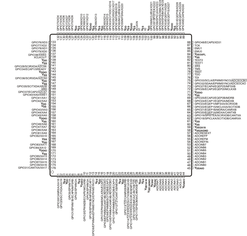 Figure 6-1 F2833x,
F2823x 176-Pin PGF/PTP LQFP (Top View)
Figure 6-1 F2833x,
F2823x 176-Pin PGF/PTP LQFP (Top View)The thermal pad should be soldered to the ground (GND) plane of the PCB because this will provide the best thermal conduction path. For this device, the thermal pad is not electrically shorted to the internal die VSS; therefore, the thermal pad does not provide an electrical connection to the PCB ground. To make optimum use of the thermal efficiencies designed into the PowerPAD™ package, the PCB must be designed with this technology in mind. A thermal land is required on the surface of the PCB directly underneath the thermal pad. The thermal land should be soldered to the thermal pad; the thermal land should be as large as needed to dissipate the required heat. An array of thermal vias should be used to connect the thermal pad to the internal GND plane of the board. See PowerPAD™ Thermally Enhanced Package for more details on using the PowerPAD package.
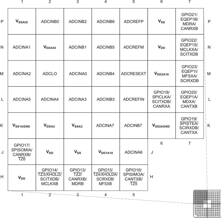 Figure 6-2 F2833x,
F2823x 179-Ball ZHH MicroStar BGA and 179-Ball ZAY nFBGA (Upper-Left Quadrant)
(Bottom View)
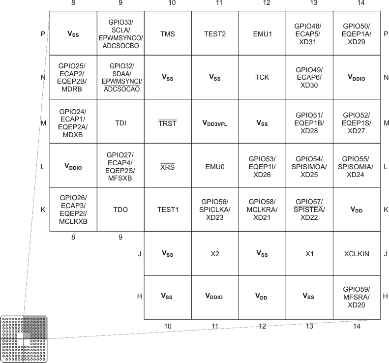 Figure 6-3 F2833x,
F2823x 179-Ball ZHH MicroStar BGA and 179-Ball ZAY nFBGA (Upper-Right Quadrant)
(Bottom View)
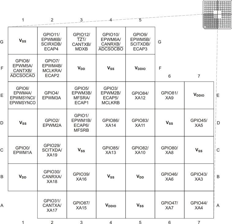 Figure 6-4 F2833x,
F2823x 179-Ball ZHH MicroStar BGA and 179-Ball ZAY nFBGA (Lower-Left Quadrant)
(Bottom View)
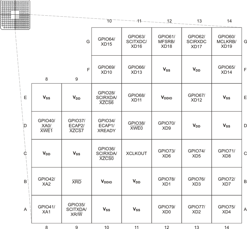 Figure 6-5 F2833x,
F2823x 179-Ball ZHH MicroStar BGA and 179-Ball ZAY nFBGA (Lower-Right Quadrant)
(Bottom View)
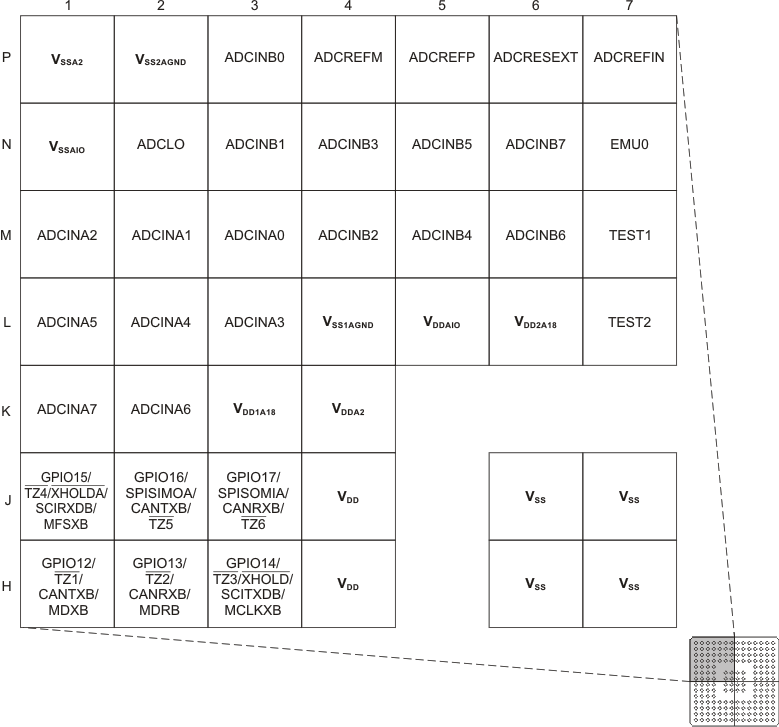 Figure 6-6 F2833x,
F2823x 176-Ball ZJZ Plastic BGA (Upper-Left Quadrant) (Bottom View)
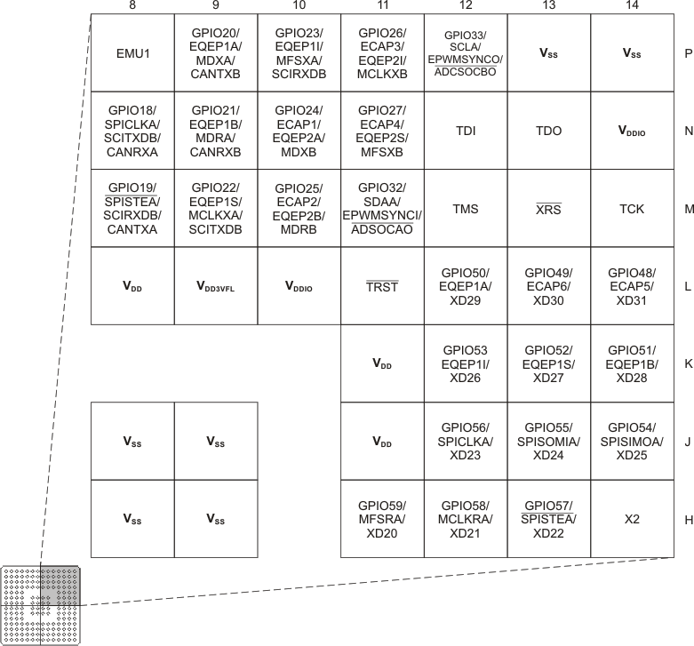 Figure 6-7 F2833x,
F2823x 176-Ball ZJZ Plastic BGA (Upper-Right Quadrant) (Bottom View)
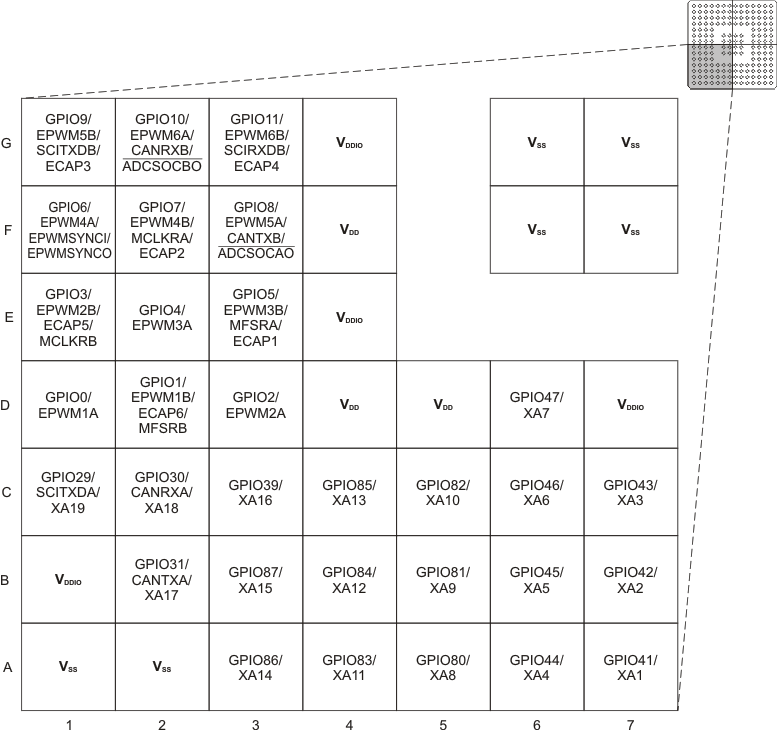 Figure 6-8 F2833x,
F2823x 176-Ball ZJZ Plastic BGA (Lower-Left Quadrant) (Bottom View)
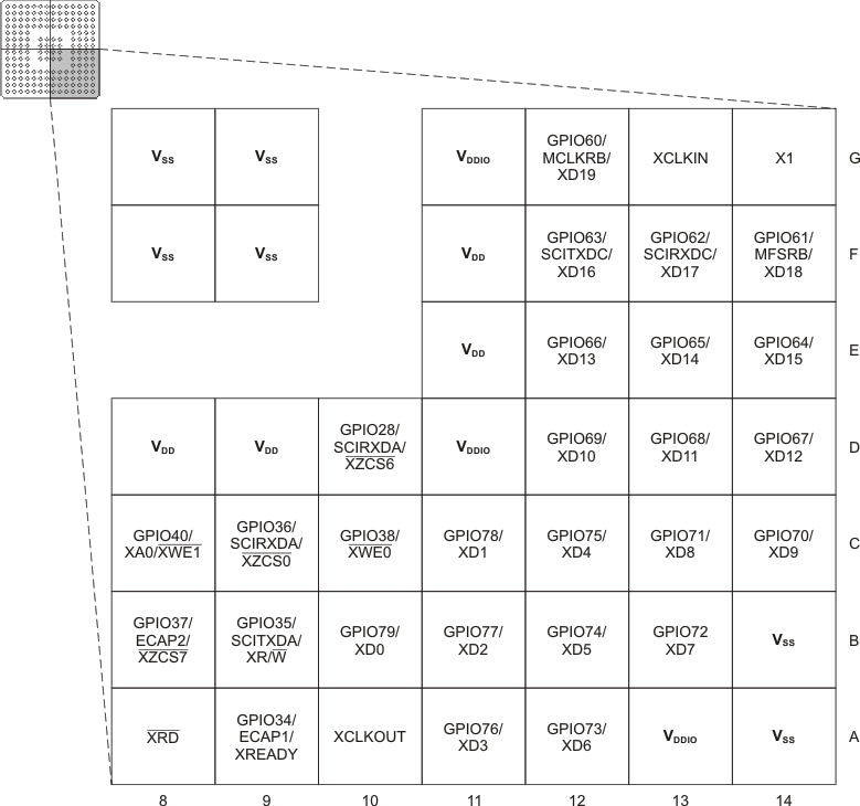 Figure 6-9 F2833x,
F2823x 176-Ball ZJZ Plastic BGA (Lower-Right Quadrant) (Bottom View)