SPRS880P December 2013 – February 2024 TMS320F28374D , TMS320F28375D , TMS320F28376D , TMS320F28377D , TMS320F28377D-Q1 , TMS320F28378D , TMS320F28379D , TMS320F28379D-Q1
PRODUCTION DATA
- 1
- 1 Features
- 2 Applications
- 3 Description
- 4 Device Comparison
- 5 Pin Configuration and Functions
-
6 Specifications
- 6.1 Absolute Maximum Ratings
- 6.2 ESD Ratings – Commercial
- 6.3 ESD Ratings – Automotive
- 6.4 Recommended Operating Conditions
- 6.5 Power Consumption Summary
- 6.6 Electrical Characteristics
- 6.7 Thermal Resistance Characteristics
- 6.8 Thermal Design Considerations
- 6.9
System
- 6.9.1 Power Sequencing
- 6.9.2 Reset Timing
- 6.9.3
Clock Specifications
- 6.9.3.1 Clock Sources
- 6.9.3.2 Clock Frequencies, Requirements, and Characteristics
- 6.9.3.3 Input Clocks and PLLs
- 6.9.3.4 XTAL Oscillator
- 6.9.3.5 Internal Oscillators
- 6.9.4 Flash Parameters
- 6.9.5 RAM Specifications
- 6.9.6 ROM Specifications
- 6.9.7 Emulation/JTAG
- 6.9.8 GPIO Electrical Data and Timing
- 6.9.9 Interrupts
- 6.9.10
Low-Power Modes
- 6.9.10.1 Clock-Gating Low-Power Modes
- 6.9.10.2 Power-Gating Low-Power Modes
- 6.9.10.3
Low-Power Mode Wakeup Timing
- 6.9.10.3.1 IDLE Mode Timing Requirements
- 6.9.10.3.2 IDLE Mode Switching Characteristics
- 6.9.10.3.3 STANDBY Mode Timing Requirements
- 6.9.10.3.4 STANDBY Mode Switching Characteristics
- 6.9.10.3.5 HALT Mode Timing Requirements
- 6.9.10.3.6 HALT Mode Switching Characteristics
- 6.9.10.3.7 HIBERNATE Mode Timing Requirements
- 6.9.10.3.8 HIBERNATE Mode Switching Characteristics
- 6.9.11 External Memory Interface (EMIF)
- 6.10
Analog Peripherals
- 6.10.1
Analog-to-Digital Converter (ADC)
- 6.10.1.1 ADC Configurability
- 6.10.1.2
ADC Electrical Data and Timing
- 6.10.1.2.1 ADC Operating Conditions (16-Bit Differential Mode)
- 6.10.1.2.2 ADC Characteristics (16-Bit Differential Mode)
- 6.10.1.2.3 ADC Operating Conditions (12-Bit Single-Ended Mode)
- 6.10.1.2.4 ADC Characteristics (12-Bit Single-Ended Mode)
- 6.10.1.2.5 ADCEXTSOC Timing Requirements
- 6.10.1.2.6 ADC Input Models
- 6.10.1.2.7 ADC Timing Diagrams
- 6.10.1.3 Temperature Sensor Electrical Data and Timing
- 6.10.2 Comparator Subsystem (CMPSS)
- 6.10.3 Buffered Digital-to-Analog Converter (DAC)
- 6.10.1
Analog-to-Digital Converter (ADC)
- 6.11
Control Peripherals
- 6.11.1 Enhanced Capture (eCAP)
- 6.11.2 Enhanced Pulse Width Modulator (ePWM)
- 6.11.3 Enhanced Quadrature Encoder Pulse (eQEP)
- 6.11.4 High-Resolution Pulse Width Modulator (HRPWM)
- 6.11.5 Sigma-Delta Filter Module (SDFM)
- 6.12
Communications Peripherals
- 6.12.1 Controller Area Network (CAN)
- 6.12.2 Inter-Integrated Circuit (I2C)
- 6.12.3 Multichannel Buffered Serial Port (McBSP)
- 6.12.4 Serial Communications Interface (SCI)
- 6.12.5 Serial Peripheral Interface (SPI)
- 6.12.6 Universal Serial Bus (USB) Controller
- 6.12.7 Universal Parallel Port (uPP) Interface
-
7 Detailed Description
- 7.1 Overview
- 7.2 Functional Block Diagram
- 7.3 Memory
- 7.4 Identification
- 7.5 Bus Architecture – Peripheral Connectivity
- 7.6 C28x Processor
- 7.7 Control Law Accelerator
- 7.8 Direct Memory Access
- 7.9 Interprocessor Communication Module
- 7.10 Boot ROM and Peripheral Booting
- 7.11 Dual Code Security Module
- 7.12 Timers
- 7.13 Nonmaskable Interrupt With Watchdog Timer (NMIWD)
- 7.14 Watchdog
- 7.15 Configurable Logic Block (CLB)
- 7.16 Functional Safety
- 8 Applications, Implementation, and Layout
- 9 Device and Documentation Support
- 10Revision History
- 11Mechanical, Packaging, and Orderable Information
Package Options
Refer to the PDF data sheet for device specific package drawings
Mechanical Data (Package|Pins)
- ZWT|337
- PTP|176
Thermal pad, mechanical data (Package|Pins)
Orderable Information
6.10.3.1.1 Buffered DAC Electrical Characteristics
| PARAMETER | TEST CONDITIONS | MIN | TYP | MAX | UNIT |
|---|---|---|---|---|---|
| Power-up time | 500(8) | µs | |||
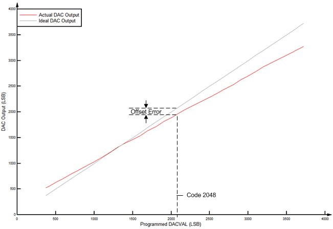
| Offset error | Midpoint | –10 | 10 | mV | |
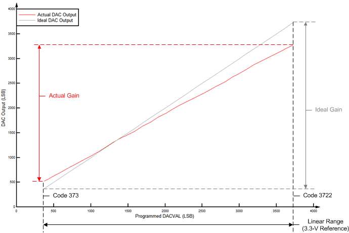
| Gain error(2) | –2.5 | 2.5 | % of FSR | ||
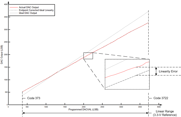
| DNL(3) | Endpoint corrected | > –1 | ±0.4 | 1 | LSB |
| INL | Endpoint corrected | –5 | ±2 | 5 | LSB |
| DACOUTx settling time | Settling to 2 LSBs after 0.3V-to-3V transition | 2 | µs | ||
| Resolution | 12 | bits | |||
| Voltage output range(4) | 0.3 | VDDA – 0.3 | V | ||
| Capacitive load | Output drive capability | 100 | pF | ||
| Resistive load | Output drive capability | 5 | kΩ | ||
| RPD pulldown resistor | 50 | kΩ | |||
| Reference voltage(5) | VDAC or VREFHI | 2.4 | 2.5 or 3.0 | VDDA | V |
| Reference input resistance(6) | VDAC or VREFHI | 170 | kΩ | ||
| Output noise | Integrated noise from 100 Hz to 100 kHz | 500 | µVrms | ||
| Noise density at 10 kHz | 711 | nVrms/√Hz | |||
| Glitch energy | 1.5 | V-ns | |||
| PSRR(7) | DC up to 1 kHz | 70 | dB | ||
| 100 kHz | 30 | ||||
| SNR | 1020 Hz | 67 | dB | ||
| THD | 1020 Hz | –63 | dB | ||
| SFDR | 1020 Hz, including harmonics and spurs | 66 | dBc | ||
| 1020 Hz, including only spurs | 104 |
The VDAC pin must be kept below VDDA + 0.3 V to ensure proper functional operation. If the VDAC pin exceeds this level, a blocking circuit may activate, and the internal value of VDAC may float to 0 V internally, giving improper DAC output.
The VREFHI pin must be kept below VDDA + 0.3 V to ensure proper functional operation. If the VREFHI pin exceeds this level, a blocking circuit may activate, and the internal value of VREFHI may float to 0 V internally, giving improper ADC conversion or DAC output.
 Figure 6-49 Buffered DAC Offset
 Figure 6-50 Buffered DAC Gain
 Figure 6-51 Buffered DAC Linearity