SPRS881K August 2014 – February 2024 TMS320F28374S , TMS320F28375S , TMS320F28375S-Q1 , TMS320F28376S , TMS320F28377S , TMS320F28377S-Q1 , TMS320F28378S , TMS320F28379S
PRODUCTION DATA
- 1
- 1 Features
- 2 Applications
- 3 Description
- 4 Device Comparison
- 5 Pin Configuration and Functions
-
6 Specifications
- 6.1 Absolute Maximum Ratings
- 6.2 ESD Ratings – Commercial
- 6.3 ESD Ratings – Automotive
- 6.4 Recommended Operating Conditions
- 6.5 Power Consumption Summary
- 6.6 Electrical Characteristics
- 6.7 Thermal Resistance Characteristics
- 6.8 Thermal Design Considerations
- 6.9
System
- 6.9.1 Power Sequencing
- 6.9.2 Reset Timing
- 6.9.3
Clock Specifications
- 6.9.3.1 Clock Sources
- 6.9.3.2 Clock Frequencies, Requirements, and Characteristics
- 6.9.3.3 Input Clocks and PLLs
- 6.9.3.4 XTAL Oscillator
- 6.9.3.5 Internal Oscillators
- 6.9.4 Flash Parameters
- 6.9.5 RAM Specifications
- 6.9.6 ROM Specifications
- 6.9.7 Emulation/JTAG
- 6.9.8 GPIO Electrical Data and Timing
- 6.9.9 Interrupts
- 6.9.10
Low-Power Modes
- 6.9.10.1 Clock-Gating Low-Power Modes
- 6.9.10.2 Power-Gating Low-Power Modes
- 6.9.10.3
Low-Power Mode Wakeup Timing
- 6.9.10.3.1 IDLE Mode Timing Requirements
- 6.9.10.3.2 IDLE Mode Switching Characteristics
- 6.9.10.3.3 STANDBY Mode Timing Requirements
- 6.9.10.3.4 STANDBY Mode Switching Characteristics
- 6.9.10.3.5 HALT Mode Timing Requirements
- 6.9.10.3.6 HALT Mode Switching Characteristics
- 6.9.10.3.7 HIBERNATE Mode Timing Requirements
- 6.9.10.3.8 HIBERNATE Mode Switching Characteristics
- 6.9.11 External Memory Interface (EMIF)
- 6.10
Analog Peripherals
- 6.10.1
Analog-to-Digital Converter (ADC)
- 6.10.1.1 ADC Configurability
- 6.10.1.2
ADC Electrical Data and Timing
- 6.10.1.2.1 ADC Operating Conditions (16-Bit Differential Mode)
- 6.10.1.2.2 ADC Characteristics (16-Bit Differential Mode)
- 6.10.1.2.3 ADC Operating Conditions (12-Bit Single-Ended Mode)
- 6.10.1.2.4 ADC Characteristics (12-Bit Single-Ended Mode)
- 6.10.1.2.5 ADCEXTSOC Timing Requirements
- 6.10.1.2.6 ADC Input Models
- 6.10.1.2.7 ADC Timing Diagrams
- 6.10.1.3 Temperature Sensor Electrical Data and Timing
- 6.10.2 Comparator Subsystem (CMPSS)
- 6.10.3 Buffered Digital-to-Analog Converter (DAC)
- 6.10.1
Analog-to-Digital Converter (ADC)
- 6.11
Control Peripherals
- 6.11.1 Enhanced Capture (eCAP)
- 6.11.2 Enhanced Pulse Width Modulator (ePWM)
- 6.11.3 Enhanced Quadrature Encoder Pulse (eQEP)
- 6.11.4 High-Resolution Pulse Width Modulator (HRPWM)
- 6.11.5 Sigma-Delta Filter Module (SDFM)
- 6.12
Communications Peripherals
- 6.12.1 Controller Area Network (CAN)
- 6.12.2 Inter-Integrated Circuit (I2C)
- 6.12.3 Multichannel Buffered Serial Port (McBSP)
- 6.12.4 Serial Communications Interface (SCI)
- 6.12.5 Serial Peripheral Interface (SPI)
- 6.12.6 Universal Serial Bus (USB) Controller
- 6.12.7 Universal Parallel Port (uPP) Interface
-
7 Detailed Description
- 7.1 Overview
- 7.2 Functional Block Diagram
- 7.3 Memory
- 7.4 Identification
- 7.5 Bus Architecture – Peripheral Connectivity
- 7.6 C28x Processor
- 7.7 Control Law Accelerator
- 7.8 Direct Memory Access
- 7.9 Boot ROM and Peripheral Booting
- 7.10 Dual Code Security Module
- 7.11 Timers
- 7.12 Nonmaskable Interrupt With Watchdog Timer (NMIWD)
- 7.13 Watchdog
- 7.14 Configurable Logic Block (CLB)
- 7.15 Functional Safety
-
8 Applications, Implementation, and Layout
- 8.1 Application and Implementation
- 8.2 Key Device Features
- 8.3 Application Information
- 9 Device and Documentation Support
- 10Revision History
- 11Mechanical, Packaging, and Orderable Information
Package Options
Refer to the PDF data sheet for device specific package drawings
Mechanical Data (Package|Pins)
- PZP|100
- ZWT|337
- PTP|176
Thermal pad, mechanical data (Package|Pins)
Orderable Information
6.10.2.1.1 Comparator Electrical Characteristics
| PARAMETER | TEST CONDITIONS | MIN | TYP | MAX | UNIT |
|---|---|---|---|---|---|
| Power-up time | 500(2) | µs | |||
| Comparator input (CMPINxx) range | 0 | VDDA | V | ||
| Input referred offset error | Low common mode, inverting input set to 50 mV | –20 | 20 | mV | |
| Hysteresis(1) | 1x | 4 | 12 | 20 | CMPSS DAC LSB |
| 2x | 17 | 24 | 33 | ||
| 3x | 25 | 36 | 50 | ||
| 4x | 30 | 48 | 67 | ||
| Response time (delay from CMPINx input change to output on ePWM X-BAR or Output X-BAR) | Step response | 21 | 60 | ns | |
| Ramp response (1.65 V/µs) | 26 | ||||
| Ramp response (8.25 mV/µs) | 30 | ||||
| Power Supply Rejection Ratio (PSRR) | Up to 250 kHz | 46 | dB | ||
| Common Mode Rejection Ratio (CMRR) | 40 | dB |
The CMPSS inputs must be kept below VDDA + 0.3 V to ensure proper functional operation. If a CMPSS input exceeds this level, an internal blocking circuit will isolate the internal comparator from the external pin until the external pin voltage returns below VDDA + 0.3 V. During this time, the internal comparator input will be floating and can decay below VDDA within approximately 0.5 µs. After this time, the comparator could begin to output an incorrect result depending on the value of the other comparator input.
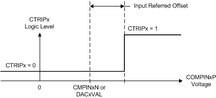
 Figure 6-43 CMPSS Comparator Input Referred Offset
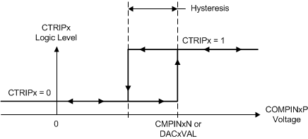
 Figure 6-44 CMPSS Comparator Hysteresis
Section 6.10.2.1.2 shows the CMPSS DAC static electrical characteristics. Figure 6-45 shows the CMPSS DAC static offset. Figure 6-46 shows the CMPSS DAC static gain. Figure 6-47 shows the CMPSS DAC static linearity.