SPRSP14E may 2019 – june 2023 TMS320F28384D , TMS320F28384D-Q1 , TMS320F28384S , TMS320F28384S-Q1 , TMS320F28386D , TMS320F28386D-Q1 , TMS320F28386S , TMS320F28386S-Q1 , TMS320F28388D , TMS320F28388S
PRODUCTION DATA
- 1
- 1 Features
- 2 Applications
- 3 Description
- 4 Revision History
- 5 Device Comparison
- 6 Terminal Configuration and Functions
-
7 Specifications
- 7.1 Absolute Maximum Ratings
- 7.2 ESD Ratings – Commercial
- 7.3 ESD Ratings – Automotive
- 7.4 Recommended Operating Conditions
- 7.5 Power Consumption Summary
- 7.6 Electrical Characteristics
- 7.7 Thermal Resistance Characteristics for ZWT Package
- 7.8 Thermal Resistance Characteristics for PTP Package
- 7.9 Thermal Design Considerations
- 7.10
System
- 7.10.1 Power Management Module (PMM)
- 7.10.2 Reset Timing
- 7.10.3
Clock Specifications
- 7.10.3.1 Clock Sources
- 7.10.3.2 Clock Frequencies, Requirements, and Characteristics
- 7.10.3.3 Input Clocks
- 7.10.3.4 XTAL Oscillator
- 7.10.3.5 Internal Oscillators
- 7.10.4 Flash Parameters
- 7.10.5 RAM Specifications
- 7.10.6 ROM Specifications
- 7.10.7 Emulation/JTAG
- 7.10.8 GPIO Electrical Data and Timing
- 7.10.9 Interrupts
- 7.10.10 Low-Power Modes
- 7.10.11 External Memory Interface (EMIF)
- 7.11
C28x Analog Peripherals
- 7.11.1 Analog Subsystem
- 7.11.2
Analog-to-Digital Converter (ADC)
- 7.11.2.1 Result Register Mapping
- 7.11.2.2 ADC Configurability
- 7.11.2.3
ADC Electrical Data and Timing
- 7.11.2.3.1 ADC Operating Conditions (16-bit Differential)
- 7.11.2.3.2 ADC Characteristics (16-bit Differential)
- 7.11.2.3.3 ADC Operating Conditions (16-bit Single-Ended)
- 7.11.2.3.4 ADC Characteristics (16-bit Single-Ended)
- 7.11.2.3.5 ADC Operating Conditions (12-bit Single-Ended)
- 7.11.2.3.6 ADC Characteristics (12-bit Single-Ended)
- 7.11.2.3.7 ADCEXTSOC Timing Requirements
- 7.11.2.3.8 ADC Input Models
- 7.11.2.3.9 ADC Timing Diagrams
- 7.11.2.4 Temperature Sensor Electrical Data and Timing
- 7.11.3 Comparator Subsystem (CMPSS)
- 7.11.4 Buffered Digital-to-Analog Converter (DAC)
- 7.12
C28x Control Peripherals
- 7.12.1 Enhanced Capture and High-Resolution Capture (eCAP, HRCAP)
- 7.12.2 Enhanced Pulse Width Modulator (ePWM)
- 7.12.3 High-Resolution Pulse Width Modulator (HRPWM)
- 7.12.4 Enhanced Quadrature Encoder Pulse (eQEP)
- 7.12.5 Sigma-Delta Filter Module (SDFM)
- 7.13
C28x Communications Peripherals
- 7.13.1 Controller Area Network (CAN)
- 7.13.2 Fast Serial Interface (FSI)
- 7.13.3 Inter-Integrated Circuit (I2C)
- 7.13.4 Multichannel Buffered Serial Port (McBSP)
- 7.13.5 Power Management Bus (PMBus)
- 7.13.6 Serial Communications Interface (SCI)
- 7.13.7 Serial Peripheral Interface (SPI)
- 7.13.8 EtherCAT Slave Controller (ESC)
- 7.13.9 Universal Serial Bus (USB) Controller
- 7.14
Connectivity Manager (CM) Peripherals
- 7.14.1 Modular Controller Area Network (MCAN) [CAN FD]
- 7.14.2 Ethernet Media Access Controller (EMAC)
- 7.14.3 Inter-Integrated Circuit (CM-I2C)
- 7.14.4 Synchronous Serial Interface (SSI)
- 7.14.5 Universal Asynchronous Receiver/Transmitter (CM-UART)
- 7.14.6 Trace Port Interface Unit (TPIU)
-
8 Detailed Description
- 8.1 Overview
- 8.2 Functional Block Diagram
- 8.3
Memory
- 8.3.1 C28x Memory Map
- 8.3.2 C28x Flash Memory Map
- 8.3.3 Peripheral Registers Memory Map
- 8.3.4 EMIF Chip Select Memory Map
- 8.3.5 CM Memory Map
- 8.3.6 CM Flash Memory Map
- 8.3.7 Peripheral Registers Memory Map (CM)
- 8.3.8
Memory Types
- 8.3.8.1 Dedicated RAM (Mx and Dx RAM)
- 8.3.8.2 Local Shared RAM (LSx RAM)
- 8.3.8.3 Global Shared RAM (GSx RAM)
- 8.3.8.4 CPU Message RAM (CPU MSGRAM)
- 8.3.8.5 CLA Message RAM (CLA MSGRAM)
- 8.3.8.6 CLA - DMA Message RAM (CLA-DMA MSGRAM)
- 8.3.8.7 CPUx - CM Message RAM (CPUx-CM MSGRAM)
- 8.3.8.8 Dedicated RAM (C0/C1 RAM)
- 8.3.8.9 Shared RAM (E0 and Sx RAM)
- 8.4 Identification
- 8.5 Bus Architecture – Peripheral Connectivity
- 8.6 Boot ROM and Peripheral Booting
- 8.7 Dual Code Security Module (DCSM)
- 8.8
C28x (CPU1/CPU2) Subsystem
- 8.8.1 C28x Processor
- 8.8.2 Embedded Real-Time Analysis and Diagnostic (ERAD)
- 8.8.3 Background CRC-32 (BGCRC)
- 8.8.4 Control Law Accelerator (CLA)
- 8.8.5 Direct Memory Access (DMA)
- 8.8.6 Interprocessor Communication (IPC) Module
- 8.8.7 C28x Timers
- 8.8.8 Dual-Clock Comparator (DCC)
- 8.8.9 Nonmaskable Interrupt With Watchdog Timer (NMIWD)
- 8.8.10 Watchdog
- 8.8.11 Configurable Logic Block (CLB)
- 8.9
Connectivity Manager (CM) Subsystem
- 8.9.1 Arm Cortex-M4 Processor
- 8.9.2 Nested Vectored Interrupt Controller (NVIC)
- 8.9.3 Advance Encryption Standard (AES) Accelerator
- 8.9.4 Generic Cyclic Redundancy Check (GCRC) Module
- 8.9.5 CM Nonmaskable Interrupt (CMNMI) Module
- 8.9.6 Memory Protection Unit (MPU)
- 8.9.7 Micro Direct Memory Access (µDMA)
- 8.9.8 Watchdog
- 8.9.9 CM Clocking
- 8.9.10 CM Timers
- 8.10 Functional Safety
- 9 Applications, Implementation, and Layout
- 10Device and Documentation Support
- 11Mechanical, Packaging, and Orderable Information
Package Options
Refer to the PDF data sheet for device specific package drawings
Mechanical Data (Package|Pins)
- ZWT|337
- PTP|176
Thermal pad, mechanical data (Package|Pins)
Orderable Information
7.13.2.1 FSI Transmitter
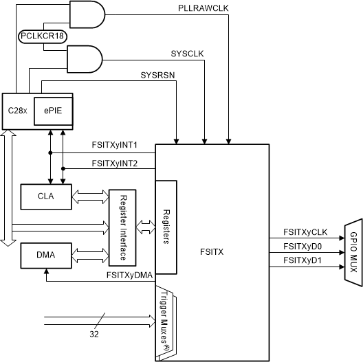
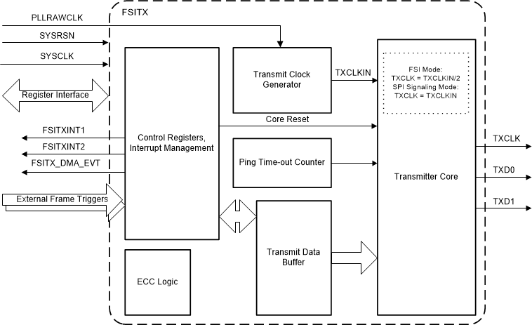
The FSI transmitter module handles the framing of data, CRC generation, signal generation of TXCLK, TXD0, and TXD1, as well as interrupt generation. The operation of the transmitter core is controlled and configured through programmable control registers. The transmitter control registers let the CPU (or the CLA) program, control, and monitor the operation of the FSI transmitter. The transmit data buffer is accessible by the CPU, CLA, and the DMA.
The transmitter has the following features:
- Automated ping frame generation
- Externally triggered ping frames
- Externally triggered data frames
- Software-configurable frame lengths
- 16-word data buffer
- Data buffer underrun and overrun detection
- Hardware-generated CRC on data bits
- Software ECC calculation on select data
- DMA support
- CLA task triggering
Figure 7-66 shows the FSITX CPU interface. Figure 7-67 shows the high-level block diagram of the FSITX. Not all data paths and internal connections are shown. This diagram provides a high-level overview of the internal modules present in the FSITX.

 Figure 7-67 FSITX Block Diagram