SPRSP85A April 2024 – September 2024 TMS320F28P550SJ , TMS320F28P559SJ-Q1
PRODMIX
- 1
- 1 Features
- 2 Applications
- 3 Description
- 4 Device Comparison
- 5 Pin Configuration and Functions
-
6 Specifications
- 6.1 Absolute Maximum Ratings
- 6.2 ESD Ratings – Commercial
- 6.3 ESD Ratings – Automotive
- 6.4 Recommended Operating Conditions
- 6.5 Power Consumption Summary
- 6.6 Electrical Characteristics
- 6.7 Special Considerations for 5V Fail-Safe Pins
- 6.8 Thermal Resistance Characteristics for PDT Package
- 6.9 Thermal Resistance Characteristics for PZ Package
- 6.10 Thermal Resistance Characteristics for PNA Package
- 6.11 Thermal Resistance Characteristics for PM Package
- 6.12 Thermal Resistance Characteristics for RSH Package
- 6.13 Thermal Design Considerations
- 6.14
System
- 6.14.1
Power Management Module (PMM)
- 6.14.1.1 Introduction
- 6.14.1.2 Overview
- 6.14.1.3 External Components
- 6.14.1.4 Power Sequencing
- 6.14.1.5 Power Management Module Electrical Data and Timing
- 6.14.2 Reset Timing
- 6.14.3
Clock Specifications
- 6.14.3.1 Clock Sources
- 6.14.3.2
Clock Frequencies, Requirements, and Characteristics
- 6.14.3.2.1
Input Clock Frequency and Timing
Requirements, PLL Lock Times
- 6.14.3.2.1.1 Input Clock Frequency
- 6.14.3.2.1.2 XTAL Oscillator Characteristics
- 6.14.3.2.1.3 X1 Input Level Characteristics When Using an External Clock Source - Not a Crystal
- 6.14.3.2.1.4 X1 Timing Requirements
- 6.14.3.2.1.5 AUXCLKIN Timing Requirements
- 6.14.3.2.1.6 APLL Characteristics
- 6.14.3.2.1.7 XCLKOUT Switching Characteristics - PLL Bypassed or Enabled
- 6.14.3.2.1.8 Internal Clock Frequencies
- 6.14.3.2.1
Input Clock Frequency and Timing
Requirements, PLL Lock Times
- 6.14.3.3 Input Clocks and PLLs
- 6.14.3.4 XTAL Oscillator
- 6.14.3.5 Internal Oscillators
- 6.14.4 Flash Parameters
- 6.14.5 RAM Specifications
- 6.14.6 ROM Specifications
- 6.14.7 Emulation/JTAG
- 6.14.8 GPIO Electrical Data and Timing
- 6.14.9 Interrupts
- 6.14.10
Low-Power Modes
- 6.14.10.1 Clock-Gating Low-Power Modes
- 6.14.10.2
Low-Power Mode Wake-up Timing
- 6.14.10.2.1 IDLE Mode Timing Requirements
- 6.14.10.2.2 IDLE Mode Switching Characteristics
- 6.14.10.2.3 IDLE Entry and Exit Timing Diagram
- 6.14.10.2.4 STANDBY Mode Timing Requirements
- 6.14.10.2.5 STANDBY Mode Switching Characteristics
- 6.14.10.2.6 STANDBY Entry and Exit Timing Diagram
- 6.14.10.2.7 HALT Mode Timing Requirements
- 6.14.10.2.8 HALT Mode Switching Characteristics
- 6.14.10.2.9 HALT Entry and Exit Timing Diagram
- 6.14.1
Power Management Module (PMM)
- 6.15
Analog Peripherals
- 6.15.1 Block Diagram
- 6.15.2 Analog Pins and Internal Connections
- 6.15.3 Analog Signal Descriptions
- 6.15.4 Analog-to-Digital Converter (ADC)
- 6.15.5 Temperature Sensor
- 6.15.6
Comparator Subsystem (CMPSS)
- 6.15.6.1 CMPx_DACL
- 6.15.6.2 CMPSS Connectivity Diagram
- 6.15.6.3 Block Diagram
- 6.15.6.4
CMPSS Electrical Data and Timing
- 6.15.6.4.1 CMPSS Comparator Electrical Characteristics
- CMPSS Comparator Input Referred Offset and Hysteresis
- 6.15.6.4.2 CMPSS DAC Static Electrical Characteristics
- 6.15.6.4.3 CMPSS Illustrative Graphs
- 6.15.6.4.4 Buffered Output from CMPx_DACL Operating Conditions
- 6.15.6.4.5 Buffered Output from CMPx_DACL Electrical Characteristics
- 6.15.7 Buffered Digital-to-Analog Converter (DAC)
- 6.15.8 Programmable Gain Amplifier (PGA)
- 6.16 Control Peripherals
- 6.17
Communications Peripherals
- 6.17.1 Modular Controller Area Network (MCAN)
- 6.17.2 Inter-Integrated Circuit (I2C)
- 6.17.3 Power Management Bus (PMBus) Interface
- 6.17.4 Serial Communications Interface (SCI)
- 6.17.5 Serial Peripheral Interface (SPI)
- 6.17.6 Local Interconnect Network (LIN)
- 6.17.7 Fast Serial Interface (FSI)
- 6.17.8 Universal Serial Bus (USB)
-
7 Detailed Description
- 7.1 Overview
- 7.2 Functional Block Diagram
- 7.3 Memory
- 7.4 Identification
- 7.5 Bus Architecture – Peripheral Connectivity
- 7.6 C28x Processor
- 7.7 Control Law Accelerator (CLA)
- 7.8 Embedded Real-Time Analysis and Diagnostic (ERAD)
- 7.9 Direct Memory Access (DMA)
- 7.10 Device Boot Modes
- 7.11 Security
- 7.12 Watchdog
- 7.13 C28x Timers
- 7.14 Dual-Clock Comparator (DCC)
- 7.15 Configurable Logic Block (CLB)
- 8 Reference Design
- 9 Device and Documentation Support
- 10Revision History
- 11Mechanical, Packaging, and Orderable Information
Refer to the PDF data sheet for device specific package drawings
Mechanical Data (Package|Pins)
- PNA|80
- PM|64
- RSH|56
- PZ|100
- PDT|128
Thermal pad, mechanical data (Package|Pins)
6.7 Special Considerations for 5V Fail-Safe Pins
GPIO2, GPIO3, GPIO9, and GPIO32 are 5V Fail-Safe (5V FS) pins on this device. This means two things:
- These pins can accept a voltage input of up to 5.5V, regardless of the supply voltage (VDDIO) level.
- These pins are also "Fail-Safe", meaning they can also have voltage applied to them prior to the device being powered.
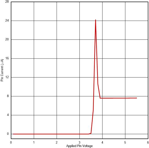
In order to achieve the above characteristics, the construction of the input buffer of these GPIOs is different from the other GPIOs on this device. As such, there is both an additional leakage current parameter defined (unpowered leakage), and a behavioral difference for the powered leakage current when the device is powered. Figure 6-1 shows the typical leakage current profile for these pins. As shown in the figure, there is an increased leakage current present as the voltage on the pin exceeds the device's supply (VDDIO) voltage. It is during this transition phase that the highest leakage current is observed. Once the input pin voltage is greater than approximately 4V, the current settles to a nominal value through the remainder of the input voltage range.
 Figure 6-1 Leakage Current vs Input Voltage
(Device Powered)