SPRSP69B July 2023 – November 2023 TMS320F28P650DK , TMS320F28P659DK-Q1
PRODMIX
- 1
- 1 Features
- 2 Applications
- 3 Description
- 4 Device Comparison
- 5 Pin Configuration and Functions
-
6 Specifications
- 6.1 Absolute Maximum Ratings
- 6.2 ESD Ratings – Commercial
- 6.3 ESD Ratings – Automotive
- 6.4 Recommended Operating Conditions
- 6.5 Power Consumption Summary
- 6.6 Electrical Characteristics
- 6.7 Thermal Resistance Characteristics for ZEJ Package
- 6.8 Thermal Resistance Characteristics for PTP Package
- 6.9 Thermal Resistance Characteristics for NMR Package
- 6.10 Thermal Resistance Characteristics for PZP Package
- 6.11 Thermal Design Considerations
- 6.12
System
- 6.12.1
Power Management Module (PMM)
- 6.12.1.1 Introduction
- 6.12.1.2 Overview
- 6.12.1.3 External Components
- 6.12.1.4 Power Sequencing
- 6.12.1.5 Power Management Module Electrical Data and Timing
- 6.12.2 Reset Timing
- 6.12.3
Clock Specifications
- 6.12.3.1 Clock Sources
- 6.12.3.2
Clock Frequencies, Requirements, and Characteristics
- 6.12.3.2.1
Input Clock Frequency and Timing
Requirements, PLL Lock Times
- 6.12.3.2.1.1 Input Clock Frequency
- 6.12.3.2.1.2 XTAL Oscillator Characteristics
- 6.12.3.2.1.3 X1 Input Level Characteristics When Using an External Clock Source Not a Crystal
- 6.12.3.2.1.4 X1 Timing Requirements
- 6.12.3.2.1.5 AUXCLKIN Timing Requirements
- 6.12.3.2.1.6 APLL Characteristics
- 6.12.3.2.1.7 XCLKOUT Switching Characteristics PLL Bypassed or Enabled
- 6.12.3.2.1.8 Internal Clock Frequencies
- 6.12.3.2.1
Input Clock Frequency and Timing
Requirements, PLL Lock Times
- 6.12.3.3 Input Clocks
- 6.12.3.4 XTAL Oscillator
- 6.12.3.5 Internal Oscillators
- 6.12.4 Flash Parameters
- 6.12.5 RAM Specifications
- 6.12.6 ROM Specifications
- 6.12.7 Emulation/JTAG
- 6.12.8 GPIO Electrical Data and Timing
- 6.12.9 Interrupts
- 6.12.10
Low-Power Modes
- 6.12.10.1 Clock-Gating Low-Power Modes
- 6.12.10.2
Low-Power Mode Wake-up Timing
- 6.12.10.2.1 IDLE Mode Timing Requirements
- 6.12.10.2.2 IDLE Mode Switching Characteristics
- 6.12.10.2.3 IDLE Entry and Exit Timing Diagram
- 6.12.10.2.4 STANDBY Mode Timing Requirements
- 6.12.10.2.5 STANDBY Mode Switching Characteristics
- 6.12.10.2.6 STANDBY Entry and Exit Timing Diagram
- 6.12.10.2.7 HALT Mode Timing Requirements
- 6.12.10.2.8 HALT Mode Switching Characteristics
- 6.12.10.2.9 HALT Entry and Exit Timing Diagram
- 6.12.11
External Memory Interface (EMIF)
- 6.12.11.1 Asynchronous Memory Support
- 6.12.11.2 Synchronous DRAM Support
- 6.12.11.3
EMIF Electrical Data and Timing
- 6.12.11.3.1 EMIF Synchronous Memory Timing Requirements
- 6.12.11.3.2 EMIF Synchronous Memory Switching Characteristics
- 6.12.11.3.3 EMIF Synchronous Memory Timing Diagrams
- 6.12.11.3.4 EMIF Asynchronous Memory Timing Requirements
- 6.12.11.3.5 EMIF Asynchronous Memory Switching Characteristics
- 6.12.11.3.6 EMIF Asynchronous Memory Timing Diagrams
- 6.12.1
Power Management Module (PMM)
- 6.13
C28x Analog Peripherals
- 6.13.1 Analog Subsystem
- 6.13.2
Analog-to-Digital Converter (ADC)
- 6.13.2.1 ADC Configurability
- 6.13.2.2
ADC Electrical Data and Timing
- 6.13.2.2.1 ADC Operating Conditions 12-bit Single-Ended
- 6.13.2.2.2 ADC Operating Conditions 12-bit Differential
- 6.13.2.2.3 ADC Operating Conditions 16-bit Single-Ended
- 6.13.2.2.4 ADC Operating Conditions 16-bit Differential
- 6.13.2.2.5 ADC Characteristics 12-bit Single-Ended
- 6.13.2.2.6 ADC Characteristics 12-bit Differential
- 6.13.2.2.7 ADC Characteristics 16-bit Single-Ended
- 6.13.2.2.8 ADC Characteristics 16-bit Differential
- 6.13.2.2.9 ADC Performance Per Pin
- 6.13.2.2.10 ADC Input Models
- 6.13.2.2.11 ADC Timing Diagrams
- 6.13.3 Temperature Sensor
- 6.13.4 Comparator Subsystem (CMPSS)
- 6.13.5 Buffered Digital-to-Analog Converter (DAC)
- 6.14
C28x Control Peripherals
- 6.14.1 Enhanced Capture (eCAP)
- 6.14.2 High-Resolution Capture (HRCAP)
- 6.14.3 Enhanced Pulse Width Modulator (ePWM)
- 6.14.4 External ADC Start-of-Conversion Electrical Data and Timing
- 6.14.5 High-Resolution Pulse Width Modulator (HRPWM)
- 6.14.6 Enhanced Quadrature Encoder Pulse (eQEP)
- 6.14.7 Sigma-Delta Filter Module (SDFM)
- 6.15
C28x Communications Peripherals
- 6.15.1 Controller Area Network (CAN)
- 6.15.2 Modular Controller Area Network (MCAN)
- 6.15.3 Fast Serial Interface (FSI)
- 6.15.4 Inter-Integrated Circuit (I2C)
- 6.15.5 Power Management Bus (PMBus) Interface
- 6.15.6 Serial Communications Interface (SCI)
- 6.15.7 Serial Peripheral Interface (SPI)
- 6.15.8 Local Interconnect Network (LIN)
- 6.15.9 EtherCAT SubordinateDevice Controller (ESC)
- 6.15.10 Universal Serial Bus (USB)
- 6.15.11 Universal Asynchronous Receiver-Transmitter (UART)
-
7 Detailed Description
- 7.1 Overview
- 7.2 Functional Block Diagram
- 7.3 Memory
- 7.4 Identification
- 7.5 Bus Architecture – Peripheral Connectivity
- 7.6 Boot ROM
- 7.7 Security
- 7.8 Advanced Encryption Standard (AES) Accelerator
- 7.9
C28x (CPU1/CPU2) Subsystem
- 7.9.1 C28x Processor
- 7.9.2 Control Law Accelerator (CLA)
- 7.9.3 Embedded Real-Time Analysis and Diagnostic (ERAD)
- 7.9.4 Background CRC-32 (BGCRC)
- 7.9.5 Direct Memory Access (DMA)
- 7.9.6 Interprocessor Communication (IPC) Module
- 7.9.7 C28x Timers
- 7.9.8 Dual-Clock Comparator (DCC)
- 7.9.9 Nonmaskable Interrupt With Watchdog Timer (NMIWD)
- 7.9.10 Watchdog
- 7.9.11 Configurable Logic Block (CLB)
- 8 Applications, Implementation, and Layout
- 9 Device and Documentation Support
- 10Revision History
- 11Mechanical, Packaging, and Orderable Information
Package Options
Refer to the PDF data sheet for device specific package drawings
Mechanical Data (Package|Pins)
- PZP|100
Thermal pad, mechanical data (Package|Pins)
Orderable Information
6.12.2 Reset Timing
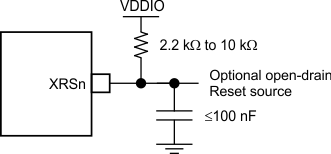
XRSn is the device reset pin. It functions as an input and open-drain output. The device has a built-in power-on reset (POR) and brown-out reset (BOR) monitors. During power up, the monitor circuits keep the XRSn pin low. For more details, see the Power Management Module (PMM) section. A watchdog or NMI watchdog reset will also drive the pin low. An external open-drain circuit may drive the pin to assert a device reset.
A resistor with a value from 2.2 kΩ to 10 kΩ should be placed between XRSn and VDDIO. A capacitor should be placed between XRSn and VSS for noise filtering, it should be 100 nF or smaller. These values will allow the watchdog to properly drive the XRSn pin to VOL within 512 OSCCLK cycles when the watchdog reset is asserted. Figure 6-19 shows the recommended reset circuit.
 Figure 6-19 Reset Circuit