SPNS254A June 2022 – March 2024 TMS570LC4357-SEP
PRODUCTION DATA
- 1
- 1 Features
- 2 Applications
- 3 Description
- 4 Device Comparison
-
5 Terminal Configuration and Functions
- 5.1 GWT BGA Package Ball-Map (337 Terminal Grid Array)
- 5.2
Terminal Functions
- 5.2.1
GWT Package
- 5.2.1.1 Multibuffered Analog-to-Digital Converters (MibADC)
- 5.2.1.2 Enhanced High-End Timer Modules (N2HET)
- 5.2.1.3 RAM Trace Port (RTP)
- 5.2.1.4 Enhanced Capture Modules (eCAP)
- 5.2.1.5 Enhanced Quadrature Encoder Pulse Modules (eQEP)
- 5.2.1.6 Enhanced Pulse-Width Modulator Modules (ePWM)
- 5.2.1.7 Data Modification Module (DMM)
- 5.2.1.8 General-Purpose Input / Output (GIO)
- 5.2.1.9 FlexRay Interface Controller (FlexRay)
- 5.2.1.10 Controller Area Network Controllers (DCAN)
- 5.2.1.11 Local Interconnect Network Interface Module (LIN)
- 5.2.1.12 Standard Serial Communication Interface (SCI)
- 5.2.1.13 Inter-Integrated Circuit Interface Module (I2C)
- 5.2.1.14 Multibuffered Serial Peripheral Interface Modules (MibSPI)
- 5.2.1.15 Ethernet Controller
- 5.2.1.16 External Memory Interface (EMIF)
- 5.2.1.17 Embedded Trace Macrocell Interface for Cortex-R5F (ETM-R5)
- 5.2.1.18 System Module Interface
- 5.2.1.19 Clock Inputs and Outputs
- 5.2.1.20 Test and Debug Modules Interface
- 5.2.1.21 Flash Supply and Test Pads
- 5.2.1.22 Supply for Core Logic: 1.2-V Nominal
- 5.2.1.23 Supply for I/O Cells: 3.3-V Nominal
- 5.2.1.24 Ground Reference for All Supplies Except VCCAD
- 5.2.1.25 Other Supplies
- 5.2.2 Multiplexing
- 5.2.1
GWT Package
-
6 Specifications
- 6.1 Absolute Maximum Ratings
- 6.2 ESD Ratings
- 6.3 Power-On Hours (POH)
- 6.4 Recommended Operating Conditions
- 6.5 Switching Characteristics Over Recommended Operating Conditions for Clock Domains
- 6.6 Wait States Required - L2 Memories
- 6.7 Power Consumption Summary
- 6.8 Input/Output Electrical Characteristics Over Recommended Operating Conditions
- 6.9 Thermal Resistance Characteristics for the BGA Package (GWT)
- 6.10 Timing and Switching Characteristics
-
7 System Information and Electrical Specifications
- 7.1 Device Power Domains
- 7.2 Voltage Monitor Characteristics
- 7.3 Power Sequencing and Power-On Reset
- 7.4 Warm Reset (nRST)
- 7.5 Arm Cortex-R5F CPU Information
- 7.6 Clocks
- 7.7 Clock Monitoring
- 7.8 Glitch Filters
- 7.9 Device Memory Map
- 7.10 Flash Memory
- 7.11 L2RAMW (Level 2 RAM Interface Module)
- 7.12 ECC / Parity Protection for Accesses to Peripheral RAMs
- 7.13 On-Chip SRAM Initialization and Testing
- 7.14 External Memory Interface (EMIF)
- 7.15 Vectored Interrupt Manager
- 7.16 ECC Error Event Monitoring and Profiling
- 7.17 DMA Controller
- 7.18 Real-Time Interrupt Module
- 7.19 Error Signaling Module
- 7.20 Reset / Abort / Error Sources
- 7.21 Digital Windowed Watchdog
- 7.22
Debug Subsystem
- 7.22.1 Block Diagram
- 7.22.2 Debug Components Memory Map
- 7.22.3 Embedded Cross Trigger
- 7.22.4 JTAG Identification Code
- 7.22.5 Debug ROM
- 7.22.6 JTAG Scan Interface Timings
- 7.22.7 Advanced JTAG Security Module
- 7.22.8 Embedded Trace Macrocell (ETM-R5)
- 7.22.9 RAM Trace Port (RTP)
- 7.22.10 Data Modification Module (DMM)
- 7.22.11 Boundary Scan Chain
-
8 Peripheral Information and Electrical Specifications
- 8.1
Enhanced Translator PWM Modules (ePWM)
- 8.1.1 ePWM Clocking and Reset
- 8.1.2 Synchronization of ePWMx Time-Base Counters
- 8.1.3 Synchronizing all ePWM Modules to the N2HET1 Module Time Base
- 8.1.4 Phase-Locking the Time-Base Clocks of Multiple ePWM Modules
- 8.1.5 ePWM Synchronization with External Devices
- 8.1.6 ePWM Trip Zones
- 8.1.7 Triggering of ADC Start of Conversion Using ePWMx SOCA and SOCB Outputs
- 8.1.8 Enhanced Translator-Pulse Width Modulator (ePWMx) Electrical Data/Timing
- 8.2 Enhanced Capture Modules (eCAP)
- 8.3 Enhanced Quadrature Encoder (eQEP)
- 8.4 12-bit Multibuffered Analog-to-Digital Converter (MibADC)
- 8.5 General-Purpose Input/Output
- 8.6 Enhanced High-End Timer (N2HET)
- 8.7 FlexRay Interface
- 8.8 Controller Area Network (DCAN)
- 8.9 Local Interconnect Network Interface (LIN)
- 8.10 Serial Communication Interface (SCI)
- 8.11 Inter-Integrated Circuit (I2C)
- 8.12 Multibuffered / Standard Serial Peripheral Interface
- 8.13 Ethernet Media Access Controller
- 8.1
Enhanced Translator PWM Modules (ePWM)
- 9 Applications, Implementation, and Layout
- 10Device and Documentation Support
- 11Revision History
- 12Mechanical, Packaging, and Orderable Information
Package Options
Refer to the PDF data sheet for device specific package drawings
Mechanical Data (Package|Pins)
- GWT|337
Thermal pad, mechanical data (Package|Pins)
Orderable Information
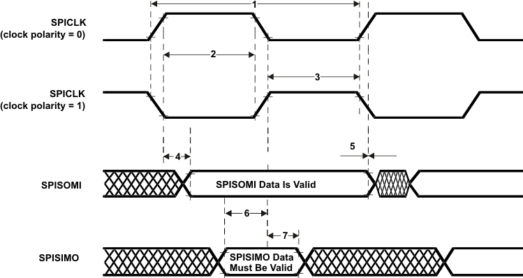
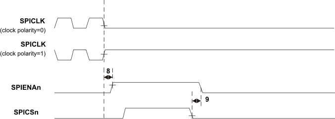
8.12.5 SPI Slave Mode I/O Timings
Table 8-40 SPI Slave Mode External Timing Parameters (CLOCK PHASE = 0, SPICLK = input, SPISIMO = input, and SPISOMI = output)(1)(2)(3)(4)
| NO. | Parameter | MIN | MAX | Unit | |
|---|---|---|---|---|---|
| 1 | tc(SPC)S | Cycle time, SPICLK(5) | 40 | ns | |
| 2(6) | tw(SPCH)S | Pulse duration, SPICLK high (clock polarity = 0) | 14 | ns | |
| tw(SPCL)S | Pulse duration, SPICLK low (clock polarity = 1) | 14 | |||
| 3(6) | tw(SPCL)S | Pulse duration, SPICLK low (clock polarity = 0) | 14 | ns | |
| tw(SPCH)S | Pulse duration, SPICLK high (clock polarity = 1) | 14 | |||
| 4(6) | td(SPCH-SOMI)S | Delay time, SPISOMI valid after SPICLK high (clock polarity = 0) | trf(SOMI) + 20 | ns | |
| td(SPCL-SOMI)S | Delay time, SPISOMI valid after SPICLK low (clock polarity = 1) | trf(SOMI) + 20 | |||
| 5(6) | th(SPCH-SOMI)S | Hold time, SPISOMI data valid after SPICLK high (clock polarity =0) | 2 | ns | |
| th(SPCL-SOMI)S | Hold time, SPISOMI data valid after SPICLK low (clock polarity =1) | 2 | |||
| 6(6) | tsu(SIMO-SPCL)S | Setup time, SPISIMO before SPICLK low (clock polarity = 0) | 4 | ns | |
| tsu(SIMO-SPCH)S | Setup time, SPISIMO before SPICLK high (clock polarity = 1) | 4 | |||
| 7(6) | th(SPCL-SIMO)S | Hold time, SPISIMO data valid after SPICLK low (clock polarity = 0) | 2 | ns | |
| th(SPCH-SIMO)S | Hold time, SPISIMO data valid after S PICLK high (clock polarity = 1) | 2 | |||
| 8 | td(SPCL-SENAH)S | Delay time, SPIENAn high after last SPICLK low (clock polarity = 0) | 1.5tc(VCLK) | 2.5tc(VCLK)+tr(ENAn)+ 22 | ns |
| td(SPCH-SENAH)S | Delay time, SPIENAn high after last SPICLK high (clock polarity = 1) | 1.5tc(VCLK) | 2.5tc(VCLK)+ tr(ENAn) + 22 | ||
| 9 | td(SCSL-SENAL)S | Delay time, SPIENAn low after SPICSn low (if new data has been written to the SPI buffer) | tf(ENAn) | tc(VCLK)+tf(ENAn)+27 | ns |
(1) The MASTER bit (SPIGCR1.0) is cleared and the CLOCK PHASE bit (SPIFMTx.16) is cleared.
(2) If the SPI is in slave mode, the following must be true: tc(SPC)S ≥ (PS + 1) tc(VCLK), where PS = prescale value set in SPIFMTx.[15:8].
(3) For rise and fall timings, see Table 6-6, Switching Characteristics for Output Timings versus Load Capacitance
(LC).
(4) tc(VCLK) = interface clock cycle time = 1 /f(VCLK)
(5) When the SPI is in Slave mode, the following must be true:
For PS values from 1 to 255: tc(SPC)S ≥ (PS +1)tc(VCLK) ≥ 40ns, where PS is the prescale value set in the SPIFMTx.[15:8] register bits.
For PS values of 0: tc(SPC)S = 2tc(VCLK) ≥ 40ns.
For PS values from 1 to 255: tc(SPC)S ≥ (PS +1)tc(VCLK) ≥ 40ns, where PS is the prescale value set in the SPIFMTx.[15:8] register bits.
For PS values of 0: tc(SPC)S = 2tc(VCLK) ≥ 40ns.
(6) The active edge of the SPICLK signal referenced is controlled by the CLOCK POLARITY bit (SPIFMTx.17).
 Figure 8-24 SPI Slave Mode External Timing (CLOCK PHASE = 0)
 Figure 8-25 SPI Slave Mode Enable Timing (CLOCK PHASE = 0)
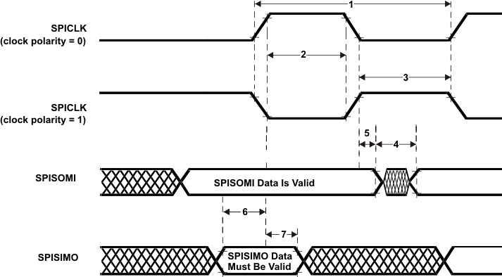
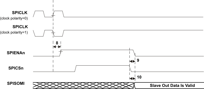
Table 8-41 SPI Slave Mode External Timing Parameters (CLOCK PHASE = 1, SPICLK = input, SPISIMO = input, and SPISOMI = output)(1)(2)(3)(4)
| NO. | Parameter | MIN | MAX | Unit | |
|---|---|---|---|---|---|
| 1 | tc(SPC)S | Cycle time, SPICLK(5) | 40 | ns | |
| 2(6) | tw(SPCH)S | Pulse duration, SPICLK high (clock polarity = 0) | 14 | ns | |
| tw(SPCL)S | Pulse duration, SPICLK low (clock polarity = 1) | 14 | |||
| 3(6) | tw(SPCL)S | Pulse duration, SPICLK low (clock polarity = 0) | 14 | ns | |
| tw(SPCH)S | Pulse duration, SPICLK high (clock polarity = 1) | 14 | |||
| 4(6) | td(SOMI-SPCL)S | Dealy time, SPISOMI data valid after SPICLK low (clock polarity = 0) | trf(SOMI) + 20 | ns | |
| td(SOMI-SPCH)S | Delay time, SPISOMI data valid after SPICLK high (clock polarity = 1) | trf(SOMI) + 20 | |||
| 5(6) | th(SPCL-SOMI)S | Hold time, SPISOMI data valid after SPICLK high (clock polarity =0) | 2 | ns | |
| th(SPCH-SOMI)S | Hold time, SPISOMI data valid after SPICLK low (clock polarity =1) | 2 | |||
| 6(6) | tsu(SIMO-SPCH)S | Setup time, SPISIMO before SPICLK high (clock polarity = 0) | 4 | ns | |
| tsu(SIMO-SPCL)S | Setup time, SPISIMO before SPICLK low (clock polarity = 1) | 4 | |||
| 7(6) | tv(SPCH-SIMO)S | High time, SPISIMO data valid after SPICLK high (clock polarity = 0) | 2 | ns | |
| tv(SPCL-SIMO)S | High time, SPISIMO data valid after SPICLK low (clock polarity = 1) | 2 | |||
| 8 | td(SPCH-SENAH)S | Delay time, SPIENAn high after last SPICLK high (clock polarity = 0) | 1.5tc(VCLK) | 2.5tc(VCLK)+tr(ENAn) + 22 | ns |
| td(SPCL-SENAH)S | Delay time, SPIENAn high after last SPICLK low (clock polarity = 1) | 1.5tc(VCLK) | 2.5tc(VCLK)+tr(ENAn) + 22 | ||
| 9 | td(SCSL-SENAL)S | Delay time, SPIENAn low after SPICSn low (if new data has been written to the SPI buffer) | tf(ENAn) | tc(VCLK)+tf(ENAn)+ 27 | ns |
| 10 | td(SCSL-SOMI)S | Delay time, SOMI valid after SPICSn low (if new data has been written to the SPI buffer) | tc(VCLK) | 2tc(VCLK)+trf(SOMI)+ 28 | ns |
(1) The MASTER bit (SPIGCR1.0) is cleared and the CLOCK PHASE bit (SPIFMTx.16) is set.
(2) If the SPI is in slave mode, the following must be true: tc(SPC)S ≤ (PS + 1) tc(VCLK), where PS = prescale value set in SPIFMTx.[15:8].
(3) For rise and fall timings, see Table 6-6, Switching Characteristics for Output Timings versus Load Capacitance
(LC).
(4) tc(VCLK) = interface clock cycle time = 1 /f(VCLK)
(5) When the SPI is in Slave mode, the following must be true:
For PS values from 1 to 255: tc(SPC)S ≥ (PS +1)tc(VCLK) ≥ 40ns, where PS is the prescale value set in the SPIFMTx.[15:8] register bits.
For PS values of 0: tc(SPC)S = 2tc(VCLK) ≥ 40ns.
For PS values from 1 to 255: tc(SPC)S ≥ (PS +1)tc(VCLK) ≥ 40ns, where PS is the prescale value set in the SPIFMTx.[15:8] register bits.
For PS values of 0: tc(SPC)S = 2tc(VCLK) ≥ 40ns.
(6) The active edge of the SPICLK signal referenced is controlled by the CLOCK POLARITY bit (SPIFMTx.17).
 Figure 8-26 SPI Slave Mode External Timing (CLOCK PHASE = 1)
 Figure 8-27 SPI Slave Mode Enable Timing (CLOCK PHASE = 1)