SPNS254A June   2022  – March 2024 TMS570LC4357-SEP

PRODUCTION DATA  

  1.   1
  2. Features
  3. Applications
  4. Description
    1. 3.1 Functional Block Diagram
  5. Device Comparison
  6. Terminal Configuration and Functions
    1. 5.1 GWT BGA Package Ball-Map (337 Terminal Grid Array)
    2. 5.2 Terminal Functions
      1. 5.2.1 GWT Package
        1. 5.2.1.1  Multibuffered Analog-to-Digital Converters (MibADC)
        2. 5.2.1.2  Enhanced High-End Timer Modules (N2HET)
        3. 5.2.1.3  RAM Trace Port (RTP)
        4. 5.2.1.4  Enhanced Capture Modules (eCAP)
        5. 5.2.1.5  Enhanced Quadrature Encoder Pulse Modules (eQEP)
        6. 5.2.1.6  Enhanced Pulse-Width Modulator Modules (ePWM)
        7. 5.2.1.7  Data Modification Module (DMM)
        8. 5.2.1.8  General-Purpose Input / Output (GIO)
        9. 5.2.1.9  FlexRay Interface Controller (FlexRay)
        10. 5.2.1.10 Controller Area Network Controllers (DCAN)
        11. 5.2.1.11 Local Interconnect Network Interface Module (LIN)
        12. 5.2.1.12 Standard Serial Communication Interface (SCI)
        13. 5.2.1.13 Inter-Integrated Circuit Interface Module (I2C)
        14. 5.2.1.14 Multibuffered Serial Peripheral Interface Modules (MibSPI)
        15. 5.2.1.15 Ethernet Controller
        16. 5.2.1.16 External Memory Interface (EMIF)
        17. 5.2.1.17 Embedded Trace Macrocell Interface for Cortex-R5F (ETM-R5)
        18. 5.2.1.18 System Module Interface
        19. 5.2.1.19 Clock Inputs and Outputs
        20. 5.2.1.20 Test and Debug Modules Interface
        21. 5.2.1.21 Flash Supply and Test Pads
        22. 5.2.1.22 Supply for Core Logic: 1.2-V Nominal
        23. 5.2.1.23 Supply for I/O Cells: 3.3-V Nominal
        24. 5.2.1.24 Ground Reference for All Supplies Except VCCAD
        25. 5.2.1.25 Other Supplies
      2. 5.2.2 Multiplexing
        1. 5.2.2.1 Output Multiplexing
          1. 5.2.2.1.1 Notes on Output Multiplexing
        2. 5.2.2.2 Input Multiplexing
          1. 5.2.2.2.1 Notes on Input Multiplexing
          2. 5.2.2.2.2 General Rules for Multiplexing Control Registers
  7. Specifications
    1. 6.1  Absolute Maximum Ratings
    2. 6.2  ESD Ratings
    3. 6.3  Power-On Hours (POH)
    4. 6.4  Recommended Operating Conditions
    5. 6.5  Switching Characteristics Over Recommended Operating Conditions for Clock Domains
    6. 6.6  Wait States Required - L2 Memories
    7. 6.7  Power Consumption Summary
    8. 6.8  Input/Output Electrical Characteristics Over Recommended Operating Conditions
    9. 6.9  Thermal Resistance Characteristics for the BGA Package (GWT)
    10. 6.10 Timing and Switching Characteristics
      1. 6.10.1 Output Buffer Drive Strengths
      2. 6.10.2 Input Timings
      3. 6.10.3 Output Timings
  8. System Information and Electrical Specifications
    1. 7.1  Device Power Domains
    2. 7.2  Voltage Monitor Characteristics
      1. 7.2.1 Important Considerations
      2. 7.2.2 Voltage Monitor Operation
      3. 7.2.3 Supply Filtering
    3. 7.3  Power Sequencing and Power-On Reset
      1. 7.3.1 Power-Up Sequence
      2. 7.3.2 Power-Down Sequence
      3. 7.3.3 Power-On Reset: nPORRST
        1. 7.3.3.1 nPORRST Electrical and Timing Requirements
    4. 7.4  Warm Reset (nRST)
      1. 7.4.1 Causes of Warm Reset
      2. 7.4.2 nRST Timing Requirements
    5. 7.5  Arm Cortex-R5F CPU Information
      1. 7.5.1 Summary of Arm Cortex-R5F CPU Features
      2. 7.5.2 Dual Core Implementation
      3.      73
      4. 7.5.3 Duplicate Clock Tree After GCLK
      5. 7.5.4 Arm Cortex-R5F CPU Compare Module (CCM) for Safety
        1. 7.5.4.1 Signal Compare Operating Modes
          1. 7.5.4.1.1 Active Compare Lockstep Mode
          2. 7.5.4.1.2 Self-Test Mode
          3. 7.5.4.1.3 Error Forcing Mode
          4. 7.5.4.1.4 Self-Test Error Forcing Mode
        2. 7.5.4.2 Bus Inactivity Monitor
        3. 7.5.4.3 CPU Registers Initialization
      6. 7.5.5 CPU Self-Test
        1. 7.5.5.1 Application Sequence for CPU Self-Test
        2. 7.5.5.2 CPU Self-Test Clock Configuration
        3. 7.5.5.3 CPU Self-Test Coverage
      7. 7.5.6 N2HET STC / LBIST Self-Test Coverage
    6. 7.6  Clocks
      1. 7.6.1 Clock Sources
        1. 7.6.1.1 Main Oscillator
          1. 7.6.1.1.1 Timing Requirements for Main Oscillator
        2. 7.6.1.2 Low-Power Oscillator
          1. 7.6.1.2.1 Features
          2.        94
          3. 7.6.1.2.2 LPO Electrical and Timing Specifications
        3. 7.6.1.3 Phase-Locked Loop (PLL) Clock Modules
          1. 7.6.1.3.1 Block Diagram
          2. 7.6.1.3.2 PLL Timing Specifications
        4. 7.6.1.4 External Clock Inputs
      2. 7.6.2 Clock Domains
        1. 7.6.2.1 Clock Domain Descriptions
        2. 7.6.2.2 Mapping of Clock Domains to Device Modules
      3. 7.6.3 Special Clock Source Selection Scheme for VCLKA4_DIVR_EMAC
      4. 7.6.4 Clock Test Mode
    7. 7.7  Clock Monitoring
      1. 7.7.1 Clock Monitor Timings
      2. 7.7.2 External Clock (ECLK) Output Functionality
      3. 7.7.3 Dual Clock Comparators
        1. 7.7.3.1 Features
        2. 7.7.3.2 Mapping of DCC Clock Source Inputs
    8. 7.8  Glitch Filters
    9. 7.9  Device Memory Map
      1. 7.9.1 Memory Map Diagram
      2. 7.9.2 Memory Map Table
      3. 7.9.3 Special Consideration for CPU Access Errors Resulting in Imprecise Aborts
      4. 7.9.4 Master/Slave Access Privileges
        1. 7.9.4.1 Special Notes on Accesses to Certain Slaves
      5. 7.9.5 MasterID to PCRx
      6. 7.9.6 CPU Interconnect Subsystem SDC MMR Port
      7. 7.9.7 Parameter Overlay Module (POM) Considerations
    10. 7.10 Flash Memory
      1. 7.10.1 Flash Memory Configuration
      2. 7.10.2 Main Features of Flash Module
      3. 7.10.3 ECC Protection for Flash Accesses
      4. 7.10.4 Flash Access Speeds
      5. 7.10.5 Flash Program and Erase Timings
        1. 7.10.5.1 Flash Program and Erase Timings for Program Flash
        2. 7.10.5.2 Flash Program and Erase Timings for Data Flash
    11. 7.11 L2RAMW (Level 2 RAM Interface Module)
      1. 7.11.1 L2 SRAM Initialization
    12. 7.12 ECC / Parity Protection for Accesses to Peripheral RAMs
    13. 7.13 On-Chip SRAM Initialization and Testing
      1. 7.13.1 On-Chip SRAM Self-Test Using PBIST
        1. 7.13.1.1 Features
        2. 7.13.1.2 PBIST RAM Groups
      2. 7.13.2 On-Chip SRAM Auto Initialization
    14. 7.14 External Memory Interface (EMIF)
      1. 7.14.1 Features
      2. 7.14.2 Electrical and Timing Specifications
        1. 7.14.2.1 Read Timing (Asynchronous RAM)
        2. 7.14.2.2 Write Timing (Asynchronous RAM)
        3. 7.14.2.3 EMIF Asynchronous Memory Timing
        4. 7.14.2.4 Read Timing (Synchronous RAM)
        5. 7.14.2.5 Write Timing (Synchronous RAM)
        6. 7.14.2.6 EMIF Synchronous Memory Timing
    15. 7.15 Vectored Interrupt Manager
      1. 7.15.1 VIM Features
      2. 7.15.2 Interrupt Generation
      3. 7.15.3 Interrupt Request Assignments
    16. 7.16 ECC Error Event Monitoring and Profiling
      1. 7.16.1 EPC Module Operation
        1. 7.16.1.1 Correctable Error Handling
        2. 7.16.1.2 Uncorrectable Error Handling
    17. 7.17 DMA Controller
      1. 7.17.1 DMA Features
      2. 7.17.2 DMA Transfer Port Assignment
      3. 7.17.3 Default DMA Request Map
      4. 7.17.4 Using a GIO terminal as a DMA Request Input
    18. 7.18 Real-Time Interrupt Module
      1. 7.18.1 Features
      2. 7.18.2 Block Diagrams
      3. 7.18.3 Clock Source Options
      4. 7.18.4 Network Time Synchronization Inputs
    19. 7.19 Error Signaling Module
      1. 7.19.1 ESM Features
      2. 7.19.2 ESM Channel Assignments
    20. 7.20 Reset / Abort / Error Sources
    21. 7.21 Digital Windowed Watchdog
    22. 7.22 Debug Subsystem
      1. 7.22.1  Block Diagram
      2. 7.22.2  Debug Components Memory Map
      3. 7.22.3  Embedded Cross Trigger
      4. 7.22.4  JTAG Identification Code
      5. 7.22.5  Debug ROM
      6. 7.22.6  JTAG Scan Interface Timings
      7. 7.22.7  Advanced JTAG Security Module
      8. 7.22.8  Embedded Trace Macrocell (ETM-R5)
        1. 7.22.8.1 ETM TRACECLKIN Selection
        2. 7.22.8.2 Timing Specifications
      9. 7.22.9  RAM Trace Port (RTP)
        1. 7.22.9.1 RTP Features
        2. 7.22.9.2 Timing Specifications
      10. 7.22.10 Data Modification Module (DMM)
        1. 7.22.10.1 DMM Features
        2. 7.22.10.2 Timing Specifications
      11. 7.22.11 Boundary Scan Chain
  9. Peripheral Information and Electrical Specifications
    1. 8.1  Enhanced Translator PWM Modules (ePWM)
      1. 8.1.1 ePWM Clocking and Reset
      2. 8.1.2 Synchronization of ePWMx Time-Base Counters
      3. 8.1.3 Synchronizing all ePWM Modules to the N2HET1 Module Time Base
      4. 8.1.4 Phase-Locking the Time-Base Clocks of Multiple ePWM Modules
      5. 8.1.5 ePWM Synchronization with External Devices
      6. 8.1.6 ePWM Trip Zones
        1. 8.1.6.1 Trip Zones TZ1n, TZ2n, TZ3n
        2. 8.1.6.2 Trip Zone TZ4n
        3. 8.1.6.3 Trip Zone TZ5n
        4. 8.1.6.4 Trip Zone TZ6n
      7. 8.1.7 Triggering of ADC Start of Conversion Using ePWMx SOCA and SOCB Outputs
      8. 8.1.8 Enhanced Translator-Pulse Width Modulator (ePWMx) Electrical Data/Timing
    2. 8.2  Enhanced Capture Modules (eCAP)
      1. 8.2.1 Clock Enable Control for eCAPx Modules
      2. 8.2.2 PWM Output Capability of eCAPx
      3. 8.2.3 Input Connection to eCAPx Modules
      4. 8.2.4 Enhanced Capture Module (eCAP) Electrical Data/Timing
    3. 8.3  Enhanced Quadrature Encoder (eQEP)
      1. 8.3.1 Clock Enable Control for eQEPx Modules
      2. 8.3.2 Using eQEPx Phase Error to Trip ePWMx Outputs
      3. 8.3.3 Input Connection to eQEPx Modules
      4. 8.3.4 Enhanced Quadrature Encoder Pulse (eQEPx) Timing
    4. 8.4  12-bit Multibuffered Analog-to-Digital Converter (MibADC)
      1. 8.4.1 MibADC Features
      2. 8.4.2 Event Trigger Options
        1. 8.4.2.1 MibADC1 Event Trigger Hookup
        2. 8.4.2.2 MibADC2 Event Trigger Hookup
        3. 8.4.2.3 Controlling ADC1 and ADC2 Event Trigger Options Using SOC Output from ePWM Modules
      3. 8.4.3 ADC Electrical and Timing Specifications
      4. 8.4.4 Performance (Accuracy) Specifications
        1. 8.4.4.1 MibADC Nonlinearity Errors
        2. 8.4.4.2 MibADC Total Error
    5. 8.5  General-Purpose Input/Output
      1. 8.5.1 Features
    6. 8.6  Enhanced High-End Timer (N2HET)
      1. 8.6.1 Features
      2. 8.6.2 N2HET RAM Organization
      3. 8.6.3 Input Timing Specifications
      4. 8.6.4 N2HET1-N2HET2 Interconnections
      5. 8.6.5 N2HET Checking
        1. 8.6.5.1 Internal Monitoring
        2. 8.6.5.2 Output Monitoring using Dual Clock Comparator (DCC)
      6. 8.6.6 Disabling N2HET Outputs
      7. 8.6.7 High-End Timer Transfer Unit (HET-TU)
        1. 8.6.7.1 Features
        2. 8.6.7.2 Trigger Connections
    7. 8.7  FlexRay Interface
      1. 8.7.1 Features
      2. 8.7.2 Electrical and Timing Specifications
      3. 8.7.3 FlexRay Transfer Unit
    8. 8.8  Controller Area Network (DCAN)
      1. 8.8.1 Features
      2. 8.8.2 241
      3. 8.8.3 Electrical and Timing Specifications
    9. 8.9  Local Interconnect Network Interface (LIN)
      1. 8.9.1 LIN Features
    10. 8.10 Serial Communication Interface (SCI)
      1. 8.10.1 Features
    11. 8.11 Inter-Integrated Circuit (I2C)
      1. 8.11.1 Features
      2. 8.11.2 I2C I/O Timing Specifications
    12. 8.12 Multibuffered / Standard Serial Peripheral Interface
      1. 8.12.1 Features
      2. 8.12.2 MibSPI Transmit and Receive RAM Organization
      3. 8.12.3 MibSPI Transmit Trigger Events
        1. 8.12.3.1 MIBSPI1 Event Trigger Hookup
        2. 8.12.3.2 MIBSPI2 Event Trigger Hookup
        3. 8.12.3.3 MIBSPI3 Event Trigger Hookup
        4. 8.12.3.4 MIBSPI4 Event Trigger Hookup
        5. 8.12.3.5 MIBSPI5 Event Trigger Hookup
      4. 8.12.4 MibSPI/SPI Master Mode I/O Timing Specifications
      5. 8.12.5 SPI Slave Mode I/O Timings
    13. 8.13 Ethernet Media Access Controller
      1. 8.13.1 Ethernet MII Electrical and Timing Specifications
      2. 8.13.2 Ethernet RMII Electrical and Timing Specifications
      3. 8.13.3 Management Data Input/Output (MDIO)
  10. Applications, Implementation, and Layout
    1. 9.1 TI Design or Reference Design
  11. 10Device and Documentation Support
    1. 10.1 Device Support
      1. 10.1.1 Development Support
      2. 10.1.2 Device and Development-Support Tool Nomenclature
    2. 10.2 Documentation Support
      1. 10.2.1 Related Documentation from Texas Instruments
      2. 10.2.2 Receiving Notification of Documentation Updates
    3. 10.3 Support Resources
    4. 10.4 Trademarks
    5. 10.5 Electrostatic Discharge Caution
    6. 10.6 Glossary
    7. 10.7 Device Identification
      1. 10.7.1 Device Identification Code Register
      2. 10.7.2 Die Identification Registers
    8. 10.8 Module Certifications
      1. 10.8.1 FlexRay Certifications
      2. 10.8.2 DCAN Certification
      3. 10.8.3 LIN Certification
        1. 10.8.3.1 LIN Master Mode
        2. 10.8.3.2 LIN Slave Mode - Fixed Baud Rate
        3. 10.8.3.3 LIN Slave Mode - Adaptive Baud Rate
  12. 11Revision History
  13. 12Mechanical, Packaging, and Orderable Information
    1. 12.1 Package Option Addendum

Package Options

Refer to the PDF data sheet for device specific package drawings

Mechanical Data (Package|Pins)
  • GWT|337
Thermal pad, mechanical data (Package|Pins)
Orderable Information

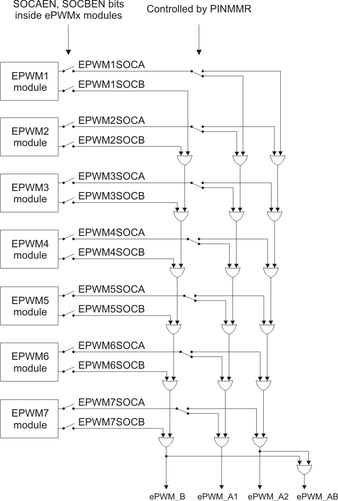
Controlling ADC1 and ADC2 Event Trigger Options Using SOC Output from ePWM Modules

As shown in Figure 8-9, the ePWMxSOCA and ePWMxSOCB outputs from each ePWM module are used to generate four signals – ePWM_B, ePWM_A1, ePWM_A2, and ePWM_AB, that are available to trigger the ADC based on the application requirement.
GUID-24A45B0D-E613-4532-A8DE-7BB1734853E5-low.gif Figure 8-9 ADC Trigger Source Generation from ePWMx
Table 8-18 Control Bit to SOC Output
CONTROL BIT SOC OUTPUT
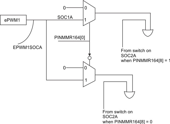
PINMMR164[0] SOC1A_SEL
PINMMR164[8] SOC2A_SEL
PINMMR164[16] SOC3A_SEL
PINMMR164[24] SOC4A_SEL
PINMMR165[0] SOC5A_SEL
PINMMR165[8] SOC6A_SEL
PINMMR165[16] SOC7A_SEL

The SOCA output from each ePWM module is connected to a "switch" shown in Figure 8-9. This switch is implemented by using the control registers in the PINMMR module. Figure 8-10 is an example of the implementation is shown for the switch on SOC1A. The switches on the other SOCA signals are implemented in the same way.
GUID-C7AF0C73-B60C-43A2-AD1F-AE85F0EDE13F-low.gif Figure 8-10 ePWM1SOC1A Switch Implementation

The logic equations for the four outputs from the combinational logic shown in Figure 8-9 are:

ePWM_B = SOC1B or SOC2B or SOC3B or SOC4B or SOC5B or SOC6B or SOC7B (1)
ePWM_A1 = [ SOC1A and not(SOC1A_SEL) ] or [ SOC2A and not(SOC2A_SEL) ] or [ SOC3A and not(SOC3A_SEL) ] or (2)
[ SOC4A and not(SOC4A_SEL) ] or [ SOC5A and not(SOC5A_SEL) ] or [ SOC6A and not(SOC6A_SEL) ] or
[ SOC7A and not(SOC7A_SEL) ]
ePWM_A2 = [ SOC1A and SOC1A_SEL ] or [ SOC2A and SOC2A_SEL ] or [ SOC3A and SOC3A_SEL ] or (3)
[ SOC4A and SOC4A_SEL ] or [ SOC5A and SOC5A_SEL ] or [ SOC6A and SOC6A_SEL ] or
[ SOC7A and SOC7A_SEL ]
ePWM_AB = ePWM_B or ePWM_A2 (4)