SPNS186C October   2012  – May 2018 TMS570LS0332 , TMS570LS0432

PRODUCTION DATA.  

  1. 1Device Overview
    1. 1.1 Features
    2. 1.2 Applications
    3. 1.3 Description
    4. 1.4 Functional Block Diagram
  2. 2Revision History
  3. 3Device Comparison
  4. 4Terminal Configuration and Functions
    1. 4.1 PZ QFP Package Pinout (100-Pin)
    2. 4.2 Terminal Functions
      1. 4.2.1  High-End Timer (N2HET)
      2. 4.2.2  Enhanced Quadrature Encoder Pulse Modules (eQEP)
      3. 4.2.3  General-Purpose Input/Output (GPIO)
      4. 4.2.4  Controller Area Network Interface Modules (DCAN1, DCAN2)
      5. 4.2.5  Multibuffered Serial Peripheral Interface (MibSPI1)
      6. 4.2.6  Standard Serial Peripheral Interface (SPI2)
      7. 4.2.7  Local Interconnect Network Controller (LIN)
      8. 4.2.8  Multibuffered Analog-to-Digital Converter (MibADC)
      9. 4.2.9  System Module
      10. 4.2.10 Error Signaling Module (ESM)
      11. 4.2.11 Main Oscillator
      12. 4.2.12 Test/Debug Interface
      13. 4.2.13 Flash
      14. 4.2.14 Core Supply
      15. 4.2.15 I/O Supply
      16. 4.2.16 Core and I/O Supply Ground Reference
    3. 4.3 Output Multiplexing and Control
      1. 4.3.1 Notes on Output Multiplexing
      2. 4.3.2 General Rules for Multiplexing Control Registers
    4. 4.4 Special Multiplexed Options
      1. 4.4.1 Filtering for eQEP Inputs
        1. 4.4.1.1 eQEPA Input
        2. 4.4.1.2 eQEPB Input
        3. 4.4.1.3 eQEPI Input
        4. 4.4.1.4 eQEPS Input
      2. 4.4.2 N2HET PIN_nDISABLE Input Port
  5. 5Specifications
    1. 5.1  Absolute Maximum Ratings
    2. 5.2  ESD Ratings
    3. 5.3  Power-On Hours (POH)
    4. 5.4  Recommended Operating Conditions
    5. 5.5  Switching Characteristics Over Recommended Operating Conditions for Clock Domains
    6. 5.6  Wait States Required
    7. 5.7  Power Consumption
    8. 5.8  Thermal Resistance Characteristics for PZ
    9. 5.9  Input/Output Electrical Characteristics
    10. 5.10 Output Buffer Drive Strengths
    11. 5.11 Input Timings
    12. 5.12 Output Timings
  6. 6System Information and Electrical Specifications
    1. 6.1  Voltage Monitor Characteristics
      1. 6.1.1 Important Considerations
      2. 6.1.2 Voltage Monitor Operation
      3. 6.1.3 Supply Filtering
    2. 6.2  Power Sequencing and Power-On Reset
      1. 6.2.1 Power-Up Sequence
      2. 6.2.2 Power-Down Sequence
      3. 6.2.3 Power-On Reset: nPORRST
        1. 6.2.3.1 nPORRST Electrical and Timing Requirements
    3. 6.3  Warm Reset (nRST)
      1. 6.3.1 Causes of Warm Reset
      2. 6.3.2 nRST Timing Requirements
    4. 6.4  ARM Cortex-R4 CPU Information
      1. 6.4.1 Summary of ARM Cortex-R4 CPU Features
      2. 6.4.2 ARM Cortex-R4 CPU Features Enabled by Software
      3. 6.4.3 Dual Core Implementation
      4. 6.4.4 Duplicate clock tree after GCLK
      5. 6.4.5 ARM Cortex-R4 CPU Compare Module (CCM) for Safety
      6. 6.4.6 CPU Self-Test
        1. 6.4.6.1 Application Sequence for CPU Self-Test
        2. 6.4.6.2 CPU Self-Test Clock Configuration
        3. 6.4.6.3 CPU Self-Test Coverage
    5. 6.5  Clocks
      1. 6.5.1 Clock Sources
        1. 6.5.1.1 Main Oscillator
          1. 6.5.1.1.1 Timing Requirements for Main Oscillator
        2. 6.5.1.2 Low-Power Oscillator
          1. 6.5.1.2.1 Features
          2. 6.5.1.2.2 LPO Electrical and Timing Specifications
        3. 6.5.1.3 Phase Locked Loop (PLL) Clock Modules
          1. 6.5.1.3.1 Block Diagram
          2. 6.5.1.3.2 PLL Timing Specifications
      2. 6.5.2 Clock Domains
        1. 6.5.2.1 Clock Domain Descriptions
        2. 6.5.2.2 Mapping of Clock Domains to Device Modules
      3. 6.5.3 Clock Test Mode
    6. 6.6  Clock Monitoring
      1. 6.6.1 Clock Monitor Timings
      2. 6.6.2 External Clock (ECLK) Output Functionality
      3. 6.6.3 Dual Clock Comparator
        1. 6.6.3.1 Features
        2. 6.6.3.2 Mapping of DCC Clock Source Inputs
    7. 6.7  Glitch Filters
    8. 6.8  Device Memory Map
      1. 6.8.1 Memory Map Diagram
      2. 6.8.2 Memory Map Table
      3. 6.8.3 Master/Slave Access Privileges
    9. 6.9  Flash Memory
      1. 6.9.1 Flash Memory Configuration
      2. 6.9.2 Main Features of Flash Module
      3. 6.9.3 ECC Protection for Flash Accesses
      4. 6.9.4 Flash Access Speeds
    10. 6.10 Flash Program and Erase Timings for Program Flash
    11. 6.11 Flash Program and Erase Timings for Data Flash
    12. 6.12 Tightly Coupled RAM Interface Module
      1. 6.12.1 Features
      2. 6.12.2 TCRAMW ECC Support
    13. 6.13 Parity Protection for Accesses to peripheral RAMs
    14. 6.14 On-Chip SRAM Initialization and Testing
      1. 6.14.1 On-Chip SRAM Self-Test Using PBIST
        1. 6.14.1.1 Features
        2. 6.14.1.2 PBIST RAM Groups
      2. 6.14.2 On-Chip SRAM Auto Initialization
    15. 6.15 Vectored Interrupt Manager
      1. 6.15.1 VIM Features
      2. 6.15.2 Interrupt Request Assignments
    16. 6.16 Real-Time Interrupt Module
      1. 6.16.1 Features
      2. 6.16.2 Block Diagrams
      3. 6.16.3 Clock Source Options
    17. 6.17 Error Signaling Module
      1. 6.17.1 Features
      2. 6.17.2 ESM Channel Assignments
    18. 6.18 Reset / Abort / Error Sources
    19. 6.19 Digital Windowed Watchdog
    20. 6.20 Debug Subsystem
      1. 6.20.1 Block Diagram
      2. 6.20.2 Debug Components Memory Map
      3. 6.20.3 JTAG Identification Code
      4. 6.20.4 Debug ROM
      5. 6.20.5 JTAG Scan Interface Timings
      6. 6.20.6 Advanced JTAG Security Module
      7. 6.20.7 Boundary Scan Chain
  7. 7Peripheral Information and Electrical Specifications
    1. 7.1 Peripheral Legend
    2. 7.2 Multibuffered 12-Bit Analog-to-Digital Converter
      1. 7.2.1 Features
      2. 7.2.2 Event Trigger Options
        1. 7.2.2.1 MIBADC Event Trigger Hookup
      3. 7.2.3 ADC Electrical and Timing Specifications
      4. 7.2.4 Performance (Accuracy) Specifications
        1. 7.2.4.1 MibADC Nonlinearity Errors
        2. 7.2.4.2 MibADC Total Error
    3. 7.3 General-Purpose Input/Output
      1. 7.3.1 Features
    4. 7.4 Enhanced High-End Timer (N2HET)
      1. 7.4.1 Features
      2. 7.4.2 N2HET RAM Organization
      3. 7.4.3 Input Timing Specifications
      4. 7.4.4 N2HET Checking
        1. 7.4.4.1 Output Monitoring using Dual Clock Comparator (DCC)
      5. 7.4.5 Disabling N2HET Outputs
      6. 7.4.6 High-End Timer Transfer Unit (N2HET)
        1. 7.4.6.1 Features
        2. 7.4.6.2 Trigger Connections
    5. 7.5 Controller Area Network (DCAN)
      1. 7.5.1 Features
      2. 7.5.2 Electrical and Timing Specifications
    6. 7.6 Local Interconnect Network Interface (LIN)
      1. 7.6.1 LIN Features
    7. 7.7 Multibuffered / Standard Serial Peripheral Interface
      1. 7.7.1 Features
      2. 7.7.2 MibSPI Transmit and Receive RAM Organization
      3. 7.7.3 MibSPI Transmit Trigger Events
        1. 7.7.3.1 MIBSPI1 Event Trigger Hookup
      4. 7.7.4 MibSPI/SPI Master Mode I/O Timing Specifications
      5. 7.7.5 SPI Slave Mode I/O Timings
    8. 7.8 Enhanced Quadrature Encoder (eQEP)
      1. 7.8.1 Clock Enable Control for eQEPx Modules
      2. 7.8.2 Using eQEPx Phase Error
      3. 7.8.3 Input Connections to eQEPx Modules
      4. 7.8.4 Enhanced Quadrature Encoder Pulse (eQEPx) Timing
  8. 8Device and Documentation Support
    1. 8.1  Device Support
      1. 8.1.1 Development Support
        1. 8.1.1.1 Getting Started
      2. 8.1.2 Device Nomenclature
    2. 8.2  Documentation Support
      1. 8.2.1 Related Documentation from Texas Instruments
    3. 8.3  Related Links
    4. 8.4  Community Resources
    5. 8.5  Trademarks
    6. 8.6  Electrostatic Discharge Caution
    7. 8.7  Glossary
    8. 8.8  Device Identification Code Register
      1. Table 8-2 Device ID Bit Allocation Register Field Descriptions
    9. 8.9  Die Identification Registers
    10. 8.10 Module Certifications
      1. 8.10.1 DCAN Certification
      2. 8.10.2 LIN Certifications
        1. 8.10.2.1 LIN Master Mode
        2. 8.10.2.2 LIN Slave Mode - Fixed Baud Rate
        3. 8.10.2.3 LIN Slave Mode - Adaptive Baud Rate
  9. 9Mechanical Packaging and Orderable Addendum
    1. 9.1 Packaging Information

Package Options

Mechanical Data (Package|Pins)
Thermal pad, mechanical data (Package|Pins)
Orderable Information

Advanced JTAG Security Module

This device includes an Advanced JTAG Security Module (AJSM), which lets the user limit JTAG access to the device after programming.
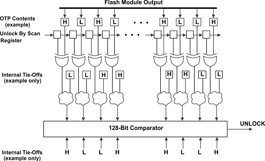
TMS570LS0432 TMS570LS0332 ajsm_unlock_pns160.gifFigure 6-16 AJSM Unlock

The device is unlocked by default by virtue of a 128-bit visible unlock code programmed in the One-Time Programmable (OTP) address 0xF000 0000.The OTP contents are XOR-ed with the contents of the Unlock-By-Scan register. The outputs of these XOR gates are again combined with a set of secret internal tie-offs. The output of this combinational logic is compared against a secret, hard-wired, 128-bit value. A match asserts the UNLOCK signal, so that the device is now unlocked.

A user can lock the device by changing bits in the visible unlock code from 1 to 0. Changing a 0 to 1 is not possible because the visible unlock code is stored in the OTP flash region. Also, changing all the 128 bits to zeros is not a valid condition and will permanently lock the device.

Once locked, a user can unlock the device by scanning an appropriate value into the Unlock-By-Scan register of the AJSM module. This register is accessible by configuring an IR value of 0b1011 on the AJSM TAP. The value to be scanned is such that the XOR of the OTP contents and the contents of the Unlock-By-Scan register results in the original visible unlock code.

The Unlock-By-Scan register is reset only by asserting power-on reset (nPORRST).

A locked device only permits JTAG accesses to the AJSM scan chain through the Secondary TAP 2 of the ICEPick module. All other secondary TAPs, test TAPs, and the boundary scan interface are not accessible in this state.