SPNS141G August   2010  – October 2018 TMS570LS10106 , TMS570LS10116 , TMS570LS10206 , TMS570LS20206 , TMS570LS20216

PRODUCTION DATA.  

  1. TMS570LS Series 16/32-BIT RISC Flash Microcontroller
    1. 1.1 Features
    2. 1.2 Description
    3. 1.3 Functional Block Diagram
  2. Device Overview
    1. 2.1 Terms and Acronyms
    2. 2.2 Device Characteristics
    3. 2.3 Memory
      1. 2.3.1 Memory Map
      2. 2.3.2 Flash Memory
      3. 2.3.3 System Modules Assignment
      4. 2.3.4 Peripheral Selects
      5. 2.3.5 Memory Auto-Initialization
      6. 2.3.6 PBIST RAM Self Test
    4. 2.4 Pin Assignments
      1. 2.4.1 PGE QFP Package Pinout (144 pin)
      2. 2.4.2 ZWT BGA Package Pinout (337 ball)
    5. 2.5 Terminal Functions
    6. 2.6 Device Support
      1. 2.6.1 Device and Development-Support Tool Nomenclature
  3. Reset / Abort Sources
    1. 3.1 Reset / Abort Sources
  4. Peripherals
    1. 4.1  Error Signaling Module (ESM)
    2. 4.2  Direct Memory Access (DMA)
    3. 4.3  High End Timer Transfer Unit (HET-TU)
    4. 4.4  Vectored Interrupt Manager (VIM)
    5. 4.5  MIBADC Event Trigger Sources
    6. 4.6  MIBSPI
      1. 4.6.1 MIBSPI Event Trigger Sources
      2. 4.6.2 MIBSPIP5/DMM Pin Multiplexing
    7. 4.7  ETM
    8. 4.8  Debug Scan Chains
      1. 4.8.1 JTAG
    9. 4.9  CCM
      1. 4.9.1 Dual Core Implementation
      2. 4.9.2 CCM-R4
    10. 4.10 LPM
    11. 4.11 Voltage Monitor
    12. 4.12 CRC
    13. 4.13 System Module Access
    14. 4.14 Debug ROM
    15. 4.15 CPU Self Test Controller: STC / LBIST
  5. Device Registers
    1. 5.1 Device Identification Code Register
      1. Table 5-1 Device ID Bit Allocation Register Field Descriptions
    2. 5.2 Die-ID Registers
    3. 5.3 PLL Registers
  6. Device Electrical Specifications
    1. 7 Operating Conditions
      1. 7.1 Absolute Maximum Ratings Over Operating Free-Air Temperature Range (unless otherwise noted)
      2. 7.2 Device Recommended Operating Conditions
      3. 7.3 Electrical Characteristics Over Operating Free-Air Temperature Range
  7. Peripheral and Electrical Specifications
    1. 8.1  Clocks
      1. 8.1.1 PLL And Clock Specifications
      2. 8.1.2 External Reference Resonator/Crystal Oscillator Clock Option
      3. 8.1.3 Validated FMPLL Setting
      4. 8.1.4 LPO And Clock Detection
      5. 8.1.5 Switching Characteristics Over Recommended Operating Conditions For Clocks
        1. 8.1.5.1 Timing - Wait States
    2. 8.2  ECLK Specification
      1. 8.2.1 Switching Characteristics Over Recommended Operating Conditions For External Clocks
    3. 8.3  RST And PORRST Timings
      1. 8.3.1 Timing Requirements For PORRST
      2. 8.3.2 Switching Characteristics Over Recommended Operating Conditions For RST
      3. 8.3.3 IO Status During PORRST
    4. 8.4  TEST Pin Timing
    5. 8.5  DAP - JTAG Scan Interface Timing
      1. 8.5.1 JTAG clock specification 12-MHz and 50-pF load on TDO output
    6. 8.6  Output Timings
      1. 8.6.1 Switching Characteristics For Output Timings Versus Load Capacitance (CL)
    7. 8.7  Input Timings
      1. 8.7.1 Timing Requirements For Input Timings
    8. 8.8  Flash Timings
    9. 8.9  SPI Master Mode Timing Parameters
      1. 8.9.1 SPI Master Mode External Timing Parameters (CLOCK PHASE = 0, SPICLK = output, SPISIMO = output, and SPISOMI = input)
      2. 8.9.2 SPI Master Mode External Timing Parameters (CLOCK PHASE = 1, SPICLK = output, SPISIMO = output, and SPISOMI = input)
    10. 8.10 SPI Slave Mode Timing Parameters
      1. 8.10.1 SPI Slave Mode External Timing Parameters (CLOCK PHASE = 0, SPICLK = input, SPISIMO = input, and SPISOMI = output)
      2. 8.10.2 SPI Slave Mode External Timing Parameters (CLOCK PHASE = 1, SPICLK = input, SPISIMO = input, and SPISOMI = output)
    11. 8.11 CAN Controller Mode Timings
      1. 8.11.1 Dynamic Characteristics For The CANnTX And CANnRX Pins
    12. 8.12 SCI/LIN Mode Timings
    13. 8.13 FlexRay Controller Mode Timings
      1. 8.13.1 Jitter Timing
    14. 8.14 EMIF Timings
      1. 8.14.1 Read Timing (Asynchronous RAM)
      2. 8.14.2 Write Timing (Asynchronous RAM)
    15. 8.15 ETM Timings
      1. 8.15.1 ETMTRACECLK Timing
      2. 8.15.2 ETMDATA Timing
    16. 8.16 RTP Timings
      1. 8.16.1 RTPCLK Timing
      2. 8.16.2 RTPDATA Timing
      3. 8.16.3 RTPENABLE Timing
    17. 8.17 DMM Timings
      1. 8.17.1 DMMCLK Timing
      2. 8.17.2 DMMDATA Timing
      3. 8.17.3 DMMENA Timing
    18. 8.18 MibADC
      1. 8.18.1 MibADC
      2. 8.18.2 MibADC Recommended Operating Conditions
      3. 8.18.3 Operating Characteristics Over Full Ranges Of Recommended Operating Conditions
      4. 8.18.4 MibADC Input Model
      5. 8.18.5 MibADC Timings
      6. 8.18.6 MibADC Nonlinearity Error
      7. 8.18.7 MibADC Total Error
  8. Revision History
  9. 10Mechanical Packaging and Orderable Information
    1. 10.1 Thermal Data
      1. 10.1.1 PGE (S-PQFP-G144) plastic Quad Flat Pack
      2. 10.1.2 ZWT (S-PBGA-N337) Plastic ball grid array
    2. 10.2 Packaging Information

Package Options

Refer to the PDF data sheet for device specific package drawings

Mechanical Data (Package|Pins)
  • ZWT|337
Thermal pad, mechanical data (Package|Pins)
Orderable Information

Device and Development-Support Tool Nomenclature

To designate the stages in the product development cycle, TI assigns prefixes to the part numbers of all devices and support tools. Each commercial family member has one of three prefixes: TMX, TMP, or TMS (e.g.,TMS570LS20216ASPGEQQ1). Texas Instruments recommends two of three possible prefix designators for its support tools: TMDX and TMDS. These prefixes represent evolutionary stages of product development from engineering prototypes (TMX/TMDX) through fully qualified production devices/tools (TMS/TMDS).

Device development evolutionary flow:

    TMX Experimental device that is not necessarily representative of the final device's electrical specifications.
    TMP Final silicon die that conforms to the device's electrical specifications but has not completed quality and reliability verification.
    TMS Fully-qualified production device.

Support tool development evolutionary flow:

    TMDX Development-support product that has not yet completed Texas Instruments internal qualification testing.
    TMDS Fully qualified development-support product.

TMX and TMP devices and TMDX development-support tools are shipped against the following disclaimer:

"Developmental product is intended for internal evaluation purposes."

TMS devices and TMDS development-support tools have been characterized fully, and the quality and reliability of the device have been demonstrated fully. TI's standard warranty applies.

Predictions show that prototype devices (TMX or TMP) have a greater failure rate than the standard production devices. Texas Instruments recommends that these devices not be used in any production system because their expected end-use failure rate still is undefined. Only qualified production devices are to be used.

TI device nomenclature also includes a suffix with the device family name. This suffix indicates the package type (for example, PGE), the temperature range (for example, "Blank" is the commercial temperature range), and the device speed range in Mega Hertz.
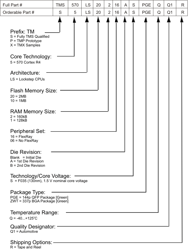
TMS570LS20216 TMS570LS20206 TMS570LS10216 TMS570LS10206 TMS570LS10116 TMS570LS10106 device_numbering_conv_pns141.gif
For actual device part numbers (P/Ns) and ordering information, see the TI website (http://www.ti.com).
Figure 2-9 Device Numbering Conventions(A)