SPNS141G August   2010  – October 2018 TMS570LS10106 , TMS570LS10116 , TMS570LS10206 , TMS570LS20206 , TMS570LS20216

PRODUCTION DATA.  

  1. TMS570LS Series 16/32-BIT RISC Flash Microcontroller
    1. 1.1 Features
    2. 1.2 Description
    3. 1.3 Functional Block Diagram
  2. Device Overview
    1. 2.1 Terms and Acronyms
    2. 2.2 Device Characteristics
    3. 2.3 Memory
      1. 2.3.1 Memory Map
      2. 2.3.2 Flash Memory
      3. 2.3.3 System Modules Assignment
      4. 2.3.4 Peripheral Selects
      5. 2.3.5 Memory Auto-Initialization
      6. 2.3.6 PBIST RAM Self Test
    4. 2.4 Pin Assignments
      1. 2.4.1 PGE QFP Package Pinout (144 pin)
      2. 2.4.2 ZWT BGA Package Pinout (337 ball)
    5. 2.5 Terminal Functions
    6. 2.6 Device Support
      1. 2.6.1 Device and Development-Support Tool Nomenclature
  3. Reset / Abort Sources
    1. 3.1 Reset / Abort Sources
  4. Peripherals
    1. 4.1  Error Signaling Module (ESM)
    2. 4.2  Direct Memory Access (DMA)
    3. 4.3  High End Timer Transfer Unit (HET-TU)
    4. 4.4  Vectored Interrupt Manager (VIM)
    5. 4.5  MIBADC Event Trigger Sources
    6. 4.6  MIBSPI
      1. 4.6.1 MIBSPI Event Trigger Sources
      2. 4.6.2 MIBSPIP5/DMM Pin Multiplexing
    7. 4.7  ETM
    8. 4.8  Debug Scan Chains
      1. 4.8.1 JTAG
    9. 4.9  CCM
      1. 4.9.1 Dual Core Implementation
      2. 4.9.2 CCM-R4
    10. 4.10 LPM
    11. 4.11 Voltage Monitor
    12. 4.12 CRC
    13. 4.13 System Module Access
    14. 4.14 Debug ROM
    15. 4.15 CPU Self Test Controller: STC / LBIST
  5. Device Registers
    1. 5.1 Device Identification Code Register
      1. Table 5-1 Device ID Bit Allocation Register Field Descriptions
    2. 5.2 Die-ID Registers
    3. 5.3 PLL Registers
  6. Device Electrical Specifications
    1. 7 Operating Conditions
      1. 7.1 Absolute Maximum Ratings Over Operating Free-Air Temperature Range (unless otherwise noted)
      2. 7.2 Device Recommended Operating Conditions
      3. 7.3 Electrical Characteristics Over Operating Free-Air Temperature Range
  7. Peripheral and Electrical Specifications
    1. 8.1  Clocks
      1. 8.1.1 PLL And Clock Specifications
      2. 8.1.2 External Reference Resonator/Crystal Oscillator Clock Option
      3. 8.1.3 Validated FMPLL Setting
      4. 8.1.4 LPO And Clock Detection
      5. 8.1.5 Switching Characteristics Over Recommended Operating Conditions For Clocks
        1. 8.1.5.1 Timing - Wait States
    2. 8.2  ECLK Specification
      1. 8.2.1 Switching Characteristics Over Recommended Operating Conditions For External Clocks
    3. 8.3  RST And PORRST Timings
      1. 8.3.1 Timing Requirements For PORRST
      2. 8.3.2 Switching Characteristics Over Recommended Operating Conditions For RST
      3. 8.3.3 IO Status During PORRST
    4. 8.4  TEST Pin Timing
    5. 8.5  DAP - JTAG Scan Interface Timing
      1. 8.5.1 JTAG clock specification 12-MHz and 50-pF load on TDO output
    6. 8.6  Output Timings
      1. 8.6.1 Switching Characteristics For Output Timings Versus Load Capacitance (CL)
    7. 8.7  Input Timings
      1. 8.7.1 Timing Requirements For Input Timings
    8. 8.8  Flash Timings
    9. 8.9  SPI Master Mode Timing Parameters
      1. 8.9.1 SPI Master Mode External Timing Parameters (CLOCK PHASE = 0, SPICLK = output, SPISIMO = output, and SPISOMI = input)
      2. 8.9.2 SPI Master Mode External Timing Parameters (CLOCK PHASE = 1, SPICLK = output, SPISIMO = output, and SPISOMI = input)
    10. 8.10 SPI Slave Mode Timing Parameters
      1. 8.10.1 SPI Slave Mode External Timing Parameters (CLOCK PHASE = 0, SPICLK = input, SPISIMO = input, and SPISOMI = output)
      2. 8.10.2 SPI Slave Mode External Timing Parameters (CLOCK PHASE = 1, SPICLK = input, SPISIMO = input, and SPISOMI = output)
    11. 8.11 CAN Controller Mode Timings
      1. 8.11.1 Dynamic Characteristics For The CANnTX And CANnRX Pins
    12. 8.12 SCI/LIN Mode Timings
    13. 8.13 FlexRay Controller Mode Timings
      1. 8.13.1 Jitter Timing
    14. 8.14 EMIF Timings
      1. 8.14.1 Read Timing (Asynchronous RAM)
      2. 8.14.2 Write Timing (Asynchronous RAM)
    15. 8.15 ETM Timings
      1. 8.15.1 ETMTRACECLK Timing
      2. 8.15.2 ETMDATA Timing
    16. 8.16 RTP Timings
      1. 8.16.1 RTPCLK Timing
      2. 8.16.2 RTPDATA Timing
      3. 8.16.3 RTPENABLE Timing
    17. 8.17 DMM Timings
      1. 8.17.1 DMMCLK Timing
      2. 8.17.2 DMMDATA Timing
      3. 8.17.3 DMMENA Timing
    18. 8.18 MibADC
      1. 8.18.1 MibADC
      2. 8.18.2 MibADC Recommended Operating Conditions
      3. 8.18.3 Operating Characteristics Over Full Ranges Of Recommended Operating Conditions
      4. 8.18.4 MibADC Input Model
      5. 8.18.5 MibADC Timings
      6. 8.18.6 MibADC Nonlinearity Error
      7. 8.18.7 MibADC Total Error
  8. Revision History
  9. 10Mechanical Packaging and Orderable Information
    1. 10.1 Thermal Data
      1. 10.1.1 PGE (S-PQFP-G144) plastic Quad Flat Pack
      2. 10.1.2 ZWT (S-PBGA-N337) Plastic ball grid array
    2. 10.2 Packaging Information

Package Options

Refer to the PDF data sheet for device specific package drawings

Mechanical Data (Package|Pins)
  • ZWT|337
Thermal pad, mechanical data (Package|Pins)
Orderable Information

Memory Map

The memory map, including all available Flash and RAM memory configurations for the device family, are shown below. Figure 2-1 applies to TMS570LS20216 and TMS570LS20206. Figure 2-2 applies to TMS570LS10216 and TMS570LS10206. Figure 2-3 applies to TMS570LS10106 and TMS570LS10116.
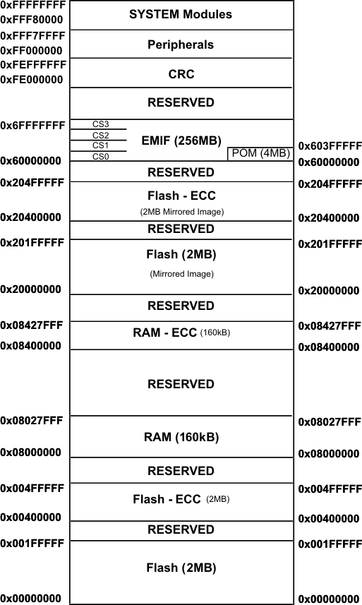
TMS570LS20216 TMS570LS20206 TMS570LS10216 TMS570LS10206 TMS570LS10116 TMS570LS10106 memory_map_202x6_pns141.gifFigure 2-1 Memory Map of TMS570LS20216 and TMS570LS20206
TMS570LS20216 TMS570LS20206 TMS570LS10216 TMS570LS10206 TMS570LS10116 TMS570LS10106 memory_map_102x6_pns141.gifFigure 2-2 Memory Map of TMS570LS10216 and TMS570LS10206
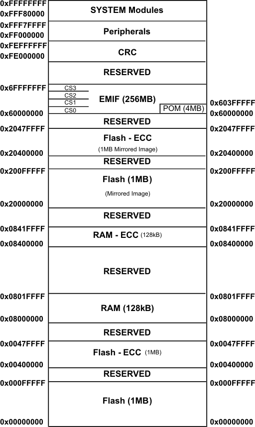
TMS570LS20216 TMS570LS20206 TMS570LS10216 TMS570LS10206 TMS570LS10116 TMS570LS10106 memory_map_101x6_pns141.gifFigure 2-3 Memory Map of TMS570LS10116 and TMS570LS10106

The Parameter Overlay memory space maps to the lower 4MB of the EMIF CS0 memory space. ECC must be disabled by software via the CPU CP15 register if POM is used to overlay the program memory to the EMIF space; otherwise ECC errors will be generated. The contents of memory connected to the EMIF are not guaranteed after a power on reset. The addressable EMIF memory range is limited to the lower 32MB of each EMIF chip select for 16bit memories, and to the lower 16MB of each EMIF chip select for 8bit memories. The default EMIF data width is 16bit. The EMIF pins do not have GIO functionality.