SCDS410D March   2019  – February 2024 TMUX1101 , TMUX1102

PRODUCTION DATA  

  1.   1
  2. Features
  3. Applications
  4. Description
  5. Device Comparison Table
  6. Pin Configuration and Functions
  7. Specifications
    1. 6.1 Absolute Maximum Ratings
    2. 6.2 ESD Ratings
    3. 6.3 Recommended Operating Conditions
    4. 6.4 Thermal Information
    5. 6.5 Electrical Characteristics (VDD = 5V ±10 %)
    6. 6.6 Electrical Characteristics (VDD = 3.3V ±10 %)
    7. 6.7 Electrical Characteristics (VDD = 1.8V ±10 %)
    8. 6.8 Electrical Characteristics (VDD = 1.2V ±10 %)
    9. 6.9 Typical Characteristics
  8. Parameter Measurement Information
    1. 7.1 On-Resistance
    2. 7.2 Off-Leakage Current
    3. 7.3 On-Leakage Current
    4. 7.4 Transition Time
    5. 7.5 Charge Injection
    6. 7.6 Off Isolation
    7. 7.7 Bandwidth
  9. Detailed Description
    1. 8.1 Overview
    2. 8.2 Functional Block Diagram
    3. 8.3 Feature Description
      1. 8.3.1 Bidirectional Operation
      2. 8.3.2 Rail-to-Rail Operation
      3. 8.3.3 1.8V Logic Compatible Inputs
      4. 8.3.4 Fail-Safe Logic
      5. 8.3.5 Ultra-Low Leakage Current
      6. 8.3.6 Ultra-Low Charge Injection
    4. 8.4 Device Functional Modes
      1. 8.4.1 Truth Tables
  10. Application and Implementation
    1. 9.1 Application Information
    2. 9.2 Typical Application - Sample-and-Hold Circuit
      1. 9.2.1 Design Requirements
      2. 9.2.2 Detailed Design Procedure
      3. 9.2.3 Application Curve
    3. 9.3 Typical Application - Switched Gain Amplifier
      1. 9.3.1 Design Requirements
      2. 9.3.2 Detailed Design Procedure
      3. 9.3.3 Application Curve
    4. 9.4 Power Supply Recommendations
    5. 9.5 Layout
      1. 9.5.1 Layout Guidelines
      2. 9.5.2 Layout Example
  11. 10Device and Documentation Support
    1. 10.1 Documentation Support
      1. 10.1.1 Related Documentation
    2. 10.2 Receiving Notification of Documentation Updates
    3. 10.3 Support Resources
    4. 10.4 Trademarks
    5. 10.5 Electrostatic Discharge Caution
    6. 10.6 Glossary
  12. 11Revision History
  13. 12Mechanical, Packaging, and Orderable Information

Package Options

Refer to the PDF data sheet for device specific package drawings

Mechanical Data (Package|Pins)
  • DBV|5
  • DCK|5
Thermal pad, mechanical data (Package|Pins)
Orderable Information

Application Curve

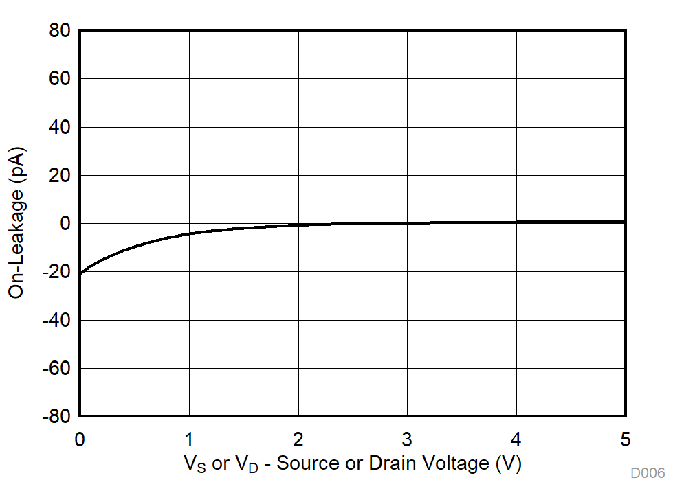
TMUX1101 and TMUX1102 have excellent charge injection performance and ultra-low leakage current, making them excellent choices to minimize sampling error for the sample-and-hold application. The charge injection and leakage performance are shown in Figure 9-2 and Figure 9-3 respectively.
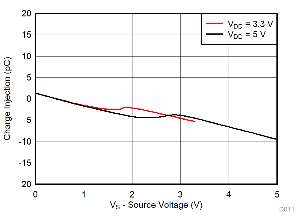
GUID-236297A5-44A2-461D-ACB3-7BF5DD6DE0EC-low.gif
TA = –40°C to +125°C
Figure 9-2 Charge Injection vs Source Voltage
GUID-D5DED5E5-304C-4724-B5D0-5246B77C8FC4-low.gif
VDD = 5V
Figure 9-3 On-Leakage vs Source or Drain Voltage