SCDS406A December 2018 – February 2024 TMUX1109
PRODUCTION DATA
- 1
- 1 Features
- 2 Applications
- 3 Description
- 4 Pin Configuration and Functions
-
5 Specifications
- 5.1 Absolute Maximum Ratings
- 5.2 ESD Ratings
- 5.3 Recommended Operating Conditions
- 5.4 Thermal Information
- 5.5 Electrical Characteristics (VDD = 5V ±10 %)
- 5.6 Electrical Characteristics (VDD = 3.3V ±10 %)
- 5.7 Electrical Characteristics (VDD = 2.5V ±10 %), (VSS = –2.5V ±10 %)
- 5.8 Electrical Characteristics (VDD = 1.8V ±10 %)
- 5.9 Electrical Characteristics (VDD = 1.2V ±10 %)
- Typical Characteristics
- 6 Detailed Description
- 7 Application and Implementation
- 8 Device and Documentation Support
- 9 Revision History
- 10Mechanical, Packaging, and Orderable Information
Package Options
Refer to the PDF data sheet for device specific package drawings
Mechanical Data (Package|Pins)
- PW|16
- RSV|16
Thermal pad, mechanical data (Package|Pins)
Orderable Information
6.1.2 Off-Leakage Current
There are two types of leakage currents associated with a switch during the off state:
- Source off-leakage current
- Drain off-leakage current
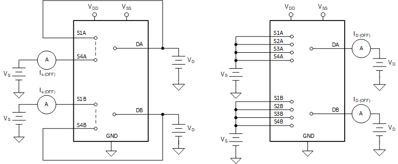
Source leakage current is defined as the leakage current flowing into or out of the source pin when the switch is off. This current is denoted by the symbol IS(OFF).
Drain leakage current is defined as the leakage current flowing into or out of the drain pin when the switch is off. This current is denoted by the symbol ID(OFF).
The setup used to measure both off-leakage currents is shown in Figure 6-2.
 Figure 6-2 Off-Leakage Measurement Setup