SCDS408C February   2019  – December 2023 TMUX1111 , TMUX1112 , TMUX1113

PRODUCTION DATA  

  1.   1
  2. Features
  3. Applications
  4. Description
  5. Device Comparison Table
  6. Pin Configuration and Functions
  7. Specifications
    1. 6.1 Absolute Maximum Ratings
    2. 6.2 ESD Ratings
    3. 6.3 Recommended Operating Conditions
    4. 6.4 Thermal Information
    5. 6.5 Electrical Characteristics (VDD = 5V ±10 %)
    6. 6.6 Electrical Characteristics (VDD = 3.3V ±10 %)
    7. 6.7 Electrical Characteristics (VDD = 1.8V ±10 %)
    8. 6.8 Electrical Characteristics (VDD = 1.2V ±10 %)
    9. 6.9 Typical Characteristics
  8. Parameter Measurement Information
    1. 7.1 On-resistance
    2. 7.2 Off-leakage current
    3. 7.3 On-leakage current
    4. 7.4 Transition time
    5. 7.5 Break-before-make
    6. 7.6 Charge injection
    7. 7.7 Off isolation
    8. 7.8 Channel-to-Channel Crosstalk
    9. 7.9 Bandwidth
  9. Detailed Description
    1. 8.1 Overview
    2. 8.2 Functional Block Diagram
    3. 8.3 Feature Description
      1. 8.3.1 Bidirectional operation
      2. 8.3.2 Rail to rail operation
      3. 8.3.3 1.8V Logic compatible inputs
      4. 8.3.4 Fail-safe logic
      5. 8.3.5 Ultra-Low Leakage Current
      6. 8.3.6 Ultra-Low Charge Injection
    4. 8.4 Device Functional Modes
    5. 8.5 Truth Tables
  10. Application and Implementation
    1. 9.1 Application Information
    2. 9.2 Typical Application - Sample-and-Hold Circuit
      1. 9.2.1 Design Requirements
      2. 9.2.2 Detailed Design Procedure
        1. 9.2.2.1 Detailed Design Procedure
      3. 9.2.3 Application Curve
    3. 9.3 Typical Application - Switched Gain Amplifier
      1. 9.3.1 Design Requirements
      2. 9.3.2 Detailed Design Procedure
      3. 9.3.3 Application Curve
    4. 9.4 Power Supply Recommendations
    5. 9.5 Layout
      1. 9.5.1 Layout Guidelines
      2. 9.5.2 Layout Example
  11. 10Device and Documentation Support
    1. 10.1 Documentation Support
      1. 10.1.1 Related Documentation
    2. 10.2 Receiving Notification of Documentation Updates
    3. 10.3 Support Resources
    4. 10.4 Trademarks
    5. 10.5 Electrostatic Discharge Caution
    6. 10.6 Glossary
  12. 11Revision History
  13. 12Mechanical, Packaging, and Orderable Information

Package Options

Refer to the PDF data sheet for device specific package drawings

Mechanical Data (Package|Pins)
  • PW|16
  • RSV|16
Thermal pad, mechanical data (Package|Pins)
Orderable Information

Ultra-Low Leakage Current

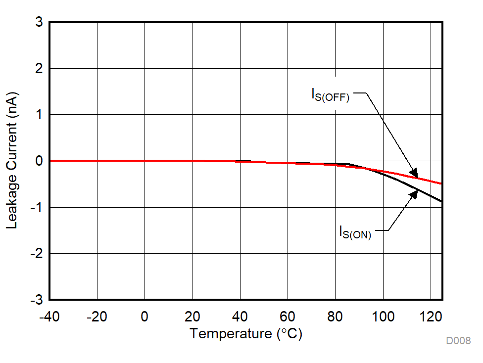
The TMUX111x devices provide extremely low on-leakage and off-leakage currents. The TMUX111x devices are capable of switching signals from high source-impedance inputs into a high input-impedance op amp with minimal offset error because of the ultra-low leakage currents. Figure 8-2 shows typical leakage currents of the TMUX111x devices versus temperature at VDD = 5V.
GUID-703F3E61-D460-491B-BBCE-F5A3481A4B99-low.gif Figure 8-2 Leakage Current vs Temperature