SCDS480 September   2024 TMUX1219-Q1

PRODUCTION DATA  

  1.   1
  2. Features
  3. Applications
  4. Description
  5. Pin Configuration and Functions
  6. Specifications
    1. 5.1 Absolute Maximum Ratings
    2. 5.2 ESD Ratings
    3. 5.3 Recommended Operating Conditions
    4. 5.4 Thermal Information
    5. 5.5 Electrical Characteristics (VDD = 5V ±10 %)
    6. 5.6 Electrical Characteristics (VDD = 3.3V ±10 %)
    7. 5.7 Electrical Characteristics (VDD = 1.8V ±10 %)
    8. 5.8 Electrical Characteristics (VDD = 1.2V ±10 %)
    9. 5.9 Typical Characteristics
  7. Parameter Measurement Information
    1. 6.1 On-Resistance
    2. 6.2 Off-Leakage Current
    3. 6.3 On-Leakage Current
    4. 6.4 Transition Time
    5. 6.5 Break-Before-Make
    6. 6.6 Charge Injection
    7. 6.7 Off Isolation
    8. 6.8 Crosstalk
    9. 6.9 Bandwidth
  8. Detailed Description
    1. 7.1 Functional Block Diagram
    2. 7.2 Feature Description
      1. 7.2.1 Bidirectional Operation
      2. 7.2.2 Rail to Rail Operation
      3. 7.2.3 1.8 V Logic Compatible Inputs
      4. 7.2.4 Fail-Safe Logic
    3. 7.3 Device Functional Modes
    4. 7.4 Truth Tables
  9. Application and Implementation
    1. 8.1 Application Information
    2. 8.2 Typical Application
      1. 8.2.1 Switchable Operational Amplifier Gain Setting
        1. 8.2.1.1 Design Requirements
        2. 8.2.1.2 Detailed Design Procedure
        3. 8.2.1.3 Application Curve
      2. 8.2.2 Input Control for Power Amplifier
        1. 8.2.2.1 Design Requirements
        2. 8.2.2.2 Detailed Design Procedure
        3. 8.2.2.3 Application Curve
  10. Power Supply Recommendations
  11. 10Layout
    1. 10.1 Layout Guidelines
      1. 10.1.1 Layout Information
    2. 10.2 Layout Example
  12. 11Device and Documentation Support
    1. 11.1 Documentation Support
      1. 11.1.1 Related Documentation
    2. 11.2 Receiving Notification of Documentation Updates
    3. 11.3 Support Resources
    4. 11.4 Trademarks
    5. 11.5 Electrostatic Discharge Caution
    6. 11.6 Glossary
  13. 12Revision History
  14. 13Mechanical, Packaging, and Orderable Information

Package Options

Mechanical Data (Package|Pins)
Thermal pad, mechanical data (Package|Pins)
Orderable Information

Input Control for Power Amplifier

Another application of the TMUX1219-Q1 is for input control of a power amplifier. Utilizing a switch allows a system to control when the DAC is connected to the power amplifier, and can stop biasing the power amplifier by switching the gate to GND. Figure 8-3 shows the TMUX1219-Q1 configured for control of the power amplifier.
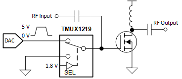
TMUX1219-Q1 Input Control of Power AmplifierFigure 8-3 Input Control of Power Amplifier