SCDS409A May   2019  – June 2020 TMUX1219

PRODUCTION DATA.  

  1. Features
  2. Applications
  3. Description
    1.     Device Images
      1.      Application Example
      2.      Block Diagram
  4. Revision History
  5. Pin Configuration and Functions
    1.     Pin Functions
  6. Specifications
    1. 6.1 Absolute Maximum Ratings
    2. 6.2 ESD Ratings
    3. 6.3 Recommended Operating Conditions
    4. 6.4 Thermal Information
    5. 6.5 Electrical Characteristics (VDD = 5 V ±10 %)
    6. 6.6 Electrical Characteristics (VDD = 3.3 V ±10 %)
    7. 6.7 Electrical Characteristics (VDD = 1.8 V ±10 %)
    8. 6.8 Electrical Characteristics (VDD = 1.2 V ±10 %)
    9. 6.9 Typical Characteristics
  7. Parameter Measurement Information
    1. 7.1 On-Resistance
    2. 7.2 Off-Leakage Current
    3. 7.3 On-Leakage Current
    4. 7.4 Transition Time
    5. 7.5 Break-Before-Make
    6. 7.6 Charge Injection
    7. 7.7 Off Isolation
    8. 7.8 Crosstalk
    9. 7.9 Bandwidth
  8. Detailed Description
    1. 8.1 Functional Block Diagram
    2. 8.2 Feature Description
      1. 8.2.1 Bidirectional Operation
      2. 8.2.2 Rail to Rail Operation
      3. 8.2.3 1.8 V Logic Compatible Inputs
      4. 8.2.4 Fail-Safe Logic
    3. 8.3 Device Functional Modes
    4. 8.4 Truth Tables
  9. Application and Implementation
    1. 9.1 Application Information
    2. 9.2 Typical Application
      1. 9.2.1 Switchable Operational Amplifier Gain Setting
        1. 9.2.1.1 Design Requirements
        2. 9.2.1.2 Detailed Design Procedure
        3. 9.2.1.3 Application Curve
      2. 9.2.2 Input Control for Power Amplifier
        1. 9.2.2.1 Design Requirements
        2. 9.2.2.2 Detailed Design Procedure
        3. 9.2.2.3 Application Curve
  10. 10Power Supply Recommendations
  11. 11Layout
    1. 11.1 Layout Guidelines
      1. 11.1.1 Layout Information
    2. 11.2 Layout Example
  12. 12Device and Documentation Support
    1. 12.1 Documentation Support
      1. 12.1.1 Related Documentation
    2. 12.2 Receiving Notification of Documentation Updates
    3. 12.3 Community Resources
    4. 12.4 Trademarks
    5. 12.5 Electrostatic Discharge Caution
    6. 12.6 Glossary
  13. 13Mechanical, Packaging, and Orderable Information

Package Options

Mechanical Data (Package|Pins)
Thermal pad, mechanical data (Package|Pins)
Orderable Information

Off-Leakage Current

Source leakage current is defined as the leakage current flowing into or out of the source pin when the switch is off. This current is denoted by the symbol IS(OFF).

The setup used to measure off-leakage current is shown in Figure 8.
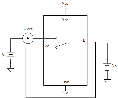
TMUX1219 Off_Leakage.gifFigure 8. Off-Leakage Measurement Setup