-
TMUX1237 3-Ω Low RON, 5-V, 2:1 (SPDT) General Purpose Switch With No Overshoot When Switching Inputs
- 1 Features
- 2 Applications
- 3 Description
- 4 Revision History
- 5 Pin Configuration and Functions
-
6 Specifications
- 6.1 Absolute Maximum Ratings
- 6.2 ESD Ratings
- 6.3 Recommended Operating Conditions
- 6.4 Thermal Information
- 6.5 Electrical Characteristics (VDD = 5 V ±10 %), GND = 0 V unless otherwise specified.
- 6.6 Electrical Characteristics (VDD = 3.3 V ±10 %), GND = 0 V unless otherwise specified.
- 6.7 Electrical Characteristics (VDD = 1.8 V ±10 %), GND = 0 V unless otherwise specified.
- 6.8 Electrical Characteristics (VDD = 1.2 V ±10 %), GND = 0 V unless otherwise specified.
- 6.9 Typical Characteristics
- 7 Parameter Measurement Information
- 8 Detailed Description
- 9 Application and Implementation
- 10Power Supply Recommendations
- 11Layout
- 12Device and Documentation Support
- 13Mechanical, Packaging, and Orderable Information
- IMPORTANT NOTICE
Package Options
Mechanical Data (Package|Pins)
- DCK|6
Thermal pad, mechanical data (Package|Pins)
Orderable Information
TMUX1237 3-Ω Low RON, 5-V, 2:1 (SPDT) General Purpose Switch With No Overshoot When Switching Inputs
1 Features
- No Overshoot When Switching Inputs
- Rail-to-rail Operation
- Bidirectional Signal Path
- 1.8 V Logic Compatible
- Fail-safe Logic
- Low On-resistance: 3 Ω
- Wide Supply Range: 1.08 V to 5.5 V
- -40°C to +125°C Operating Temperature
- Low Supply Current: 7 nA
- Break-before-make Switching
- ESD Protection HBM: 2000 V
2 Applications
- Analog and Digital Switching
- I2C and SPI Bus Multiplexing
- Remote Radio Units (RRU)
- Active Antenna System mMIMO (AAS)
- Rack Server
- Network Interface Card (NIC)
- Barcode Scanner
- Building Automation
- Analog Input Module
- Motor Drives
- Video Surveillance
- Electronic Point of Sale
- Desktop PC
- Appliances
3 Description
The TMUX1237 is a general purpose 2:1, single-pole double-throw (SPDT), switch that supports a wide operating range of 1.08 V to 5.5 V. The device supports bidirectional analog and digital signals on the source (Sx) and drain (D) pins ranging from GND to VDD. The state of the select pin (SEL) controls which of the two sources pins are connected to the drain pin. Additionally, the TMUX1237 has a low supply current of 7 nA which enables the device to be used in a host of handheld or low power applications.
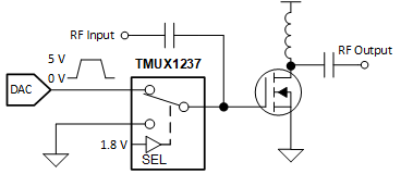
The TMUX1237 improves system reliability by eliminating overshoot that might occur in a system due to switching between two voltage levels on the source (Sx) pins. In addition, the TMUX1237 also maintains fast switching times, enabling it to improve system performance for a wide range of applications from communications equipment to building automation.
All logic inputs have 1.8 V logic compatible thresholds, ensuring both TTL and CMOS logic compatibility when operating in the valid supply voltage range. Fail-Safe Logic circuitry allows voltages on the control pins to be applied before the supply pin, protecting the device from potential damage.
Device Information(1)
| PART NUMBER | PACKAGE | BODY SIZE (NOM) |
|---|---|---|
| TMUX1237 | SC70 (6) | 2.00 mm × 1.25 mm |
- For all available packages, see the package option addendum at the end of the data sheet.
SPACER
SPACER
Device Images
TMUX1237 Block Diagram

Application Example
4 Revision History
Changes from * Revision (Decemeber 2019) to A Revision
- Changed the document status From: Product Preview To: Production DataGo
5 Pin Configuration and Functions
Pin Functions
| PIN | TYPE(1) | DESCRIPTION(2) | |
|---|---|---|---|
| NAME | NO. | ||
| S2 | 1 | I/O | Source pin 2. Can be an input or output. |
| VDD | 2 | P | Positive power supply. This pin is the most positive power-supply potential. For reliable operation, connect a decoupling capacitor ranging from 0.1 µF to 10 µF between VDD and GND. |
| S1 | 3 | I/O | Source pin 1. Can be an input or output. |
| D | 4 | I/O | Drain pin. Can be an input or output. |
| GND | 5 | P | Ground (0 V) reference |
| SEL | 6 | I | Select pin: controls state of the switch according to Table 1. (Logic Low = S1 to D, Logic High = S2 to D) |
6 Specifications
6.1 Absolute Maximum Ratings
Over operating free-air temperature range (unless otherwise noted).(1)(2)(3)| MIN | MAX | UNIT | ||
|---|---|---|---|---|
| VDD | Supply voltage | –0.5 | 6 | V |
| VSEL or VEN | Logic control input pin voltage (SEL) | –0.5 | 6 | V |
| ISEL or IEN | Logic control input pin current (SEL) | –30 | 30 | mA |
| VS or VD | Source or drain voltage (Sx, D) | –0.5 | VDD+0.5 | V |
| IS or ID (CONT) | Source or drain continuous current (Sx, D) | –50 | 50 | mA |
| IK | Diode clamp current(4) | –30 | 30 | mA |
| Tstg | Storage temperature | –65 | 150 | °C |
| TJ | Junction temperature | 150 | °C | |
6.2 ESD Ratings
| VALUE | UNIT | |||
|---|---|---|---|---|
| V(ESD) | Electrostatic discharge | Human body model (HBM), per ANSI/ESDA/JEDEC JS-001, all pins(1) | ±2000 | V |
| Charged device model (CDM), per JEDEC specification JESD22-C101, all pins(2) | ±750 | |||
6.3 Recommended Operating Conditions
Over operating free-air temperature range (unless otherwise noted).| MIN | NOM | MAX | UNIT | ||
|---|---|---|---|---|---|
| VDD | Supply voltage | 1.08 | 5.5 | V | |
| VS or VD | Signal path input/output voltage (source or drain pin) (Sx, D) | 0 | VDD | V | |
| VSEL | Logic control input pin voltage (SEL) | 0 | 5.5 | V | |
| IS or ID | Signal path continuous current (source or drain pins: Sx, D) | –50 | 50 | mA | |
| TA | Ambient temperature | –40 | 125 | °C | |
6.4 Thermal Information
| THERMAL METRIC(1) | TMUX1237 | UNIT | |
|---|---|---|---|
| SC70 (DCK) | |||
| 6 PINS | |||
| RθJA | Junction-to-ambient thermal resistance | 243.6 | °C/W |
| RθJC(top) | Junction-to-case (top) thermal resistance | 180.9 | °C/W |
| RθJB | Junction-to-board thermal resistance | 106.3 | °C/W |
| ΨJT | Junction-to-top characterization parameter | 89.1 | °C/W |
| ΨJB | Junction-to-board characterization parameter | 106.0 | °C/W |
| RθJC(bot) | Junction-to-case (bottom) thermal resistance | N/A | °C/W |
6.5 Electrical Characteristics (VDD = 5 V ±10 %), GND = 0 V unless otherwise specified.
At TA = 25°C, VDD = 5 V (unless otherwise noted).| PARAMETER | TEST CONDITIONS | TA | MIN | TYP | MAX | UNIT | |
|---|---|---|---|---|---|---|---|
| ANALOG SWITCH | |||||||
| RON | On-resistance | VS = 0 V to VDD
ISD = 10 mA Refer to On-Resistance |
25°C | 3 | Ω | ||
| –40°C to +85°C | 5 | Ω | |||||
| –40°C to +125°C | 5 | Ω | |||||
| ΔRON | On-resistance matching between channels | VS = 0 V to VDD
ISD = 10 mA Refer to On-Resistance |
25°C | 0.15 | Ω | ||
| –40°C to +85°C | 1 | Ω | |||||
| –40°C to +125°C | 1 | Ω | |||||
| RON FLAT | On-resistance flatness | VS = 0 V to VDD
ISD = 10 mA Refer to On-Resistance |
25°C | 1.5 | Ω | ||
| –40°C to +85°C | 2 | Ω | |||||
| –40°C to +125°C | 3 | Ω | |||||
| IS(OFF) | Source off leakage current(1) | VDD = 5 V
Switch Off VD = 4.5 V / 1.5 V VS = 1.5 V / 4.5 V Refer to Off-Leakage Current |
25°C | ±75 | nA | ||
| –40°C to +85°C | –150 | 150 | nA | ||||
| –40°C to +125°C | –175 | 175 | nA | ||||
| ID(ON)
IS(ON) |
Channel on leakage current | VDD = 5 V
Switch On VD = VS = 4.5 V / 1 V Refer to On-Leakage Current |
25°C | ±200 | nA | ||
| –40°C to +85°C | –500 | 500 | nA | ||||
| –40°C to +125°C | –750 | 750 | nA | ||||
| LOGIC INPUTS | |||||||
| VIH | Input logic high | -40°C to 125°C | 1.32 | 5.5 | V | ||
| VIL | Input logic low | -40°C to 125°C | 0 | 0.87 | V | ||
| IIH
IIL |
Input leakage current | 25°C | ±0.005 | µA | |||
| IIH
IIL |
Input leakage current | –40°C to +125°C | ±0.05 | µA | |||
| CIN | Digital input capacitance | 25°C | 1 | pF | |||
| CIN | Digital input capacitance | –40°C to +125°C | 2 | pF | |||
| POWER SUPPLY | |||||||
| IDD | VDD supply current | Digital Inputs = 0 V or 5.5 V | 25°C | 0.007 | µA | ||
| –40°C to +125°C | 2.6 | µA | |||||
| DYNAMIC CHARACTERISTICS | |||||||
| tTRAN | Switching time between channels | VS = 3 V
RL = 200 Ω, CL = 15 pF |
25°C | 12 | ns | ||
| –40°C to +85°C | 19 | ns | |||||
| –40°C to +125°C | 20 | ns | |||||
| tOPEN (BBM) | Break before make time | VS = 3 V
RL = 200 Ω, CL = 15 pF |
25°C | 40 | ns | ||
| –40°C to +85°C | 1 | ns | |||||
| –40°C to +125°C | 1 | ns | |||||
| QC | Charge Injection | VS = VDD /2
RS = 0 Ω, CL = 1 nF |
25°C | –10 | pC | ||
| OISO | Off Isolation | RL = 50 Ω, CL = 5 pF
f = 1 MHz |
25°C | –65 | dB | ||
| RL = 50 Ω, CL = 5 pF
f = 10 MHz |
25°C | –45 | dB | ||||
| XTALK | Crosstalk | RL = 50 Ω, CL = 5 pF
f = 1 MHz |
25°C | –65 | dB | ||
| RL = 50 Ω, CL = 5 pF
f = 10 MHz |
25°C | –45 | dB | ||||
| BW | Bandwidth | RL = 50 Ω, CL = 5 pF | 25°C | 400 | MHz | ||
| CSOFF | Source off capacitance | f = 1 MHz | 25°C | 8 | pF | ||
| CSON
CDON |
On capacitance | f = 1 MHz | 25°C | 21 | pF | ||
6.6 Electrical Characteristics (VDD = 3.3 V ±10 %), GND = 0 V unless otherwise specified.
At TA = 25°C, VDD = 3.3 V (unless otherwise noted).| PARAMETER | TEST CONDITIONS | TA | MIN | TYP | MAX | UNIT | |
|---|---|---|---|---|---|---|---|
| ANALOG SWITCH | |||||||
| RON | On-resistance | VS = 0 V to VDD
ISD = 10 mA Refer to On-Resistance |
25°C | 4.5 | Ω | ||
| –40°C to +85°C | 12.5 | Ω | |||||
| –40°C to +125°C | 13 | Ω | |||||
| ΔRON | On-resistance matching between channels | VS = 0 V to VDD
ISD = 10 mA Refer to On-Resistance |
25°C | 0.15 | Ω | ||
| –40°C to +85°C | 1 | Ω | |||||
| –40°C to +125°C | 1 | Ω | |||||
| RON FLAT | On-resistance flatness | VS = 0 V to VDD
ISD = 10 mA Refer to On-Resistance |
25°C | 3.5 | Ω | ||
| –40°C to +85°C | 4 | Ω | |||||
| –40°C to +125°C | 5 | Ω | |||||
| IS(OFF) | Source off leakage current(1) | VDD = 3.3 V
Switch Off VD = 3 V / 1 V VS = 1 V / 3 V Refer to Off-Leakage Current |
25°C | ±75 | nA | ||
| –40°C to +85°C | –150 | 150 | nA | ||||
| –40°C to +125°C | –175 | 175 | nA | ||||
| ID(ON)
IS(ON) |
Channel on leakage current | VDD = 3.3 V
Switch On VD = VS = 3 V / 1 V Refer to On-Leakage Current |
25°C | ±200 | nA | ||
| –40°C to +85°C | –500 | 500 | nA | ||||
| –40°C to +125°C | –750 | 750 | nA | ||||
| LOGIC INPUTS | |||||||
| VIH | Input logic high | -40°C to 125°C | 1.25 | 5.5 | V | ||
| VIL | Input logic low | -40°C to 125°C | 0 | 0.8 | V | ||
| IIH
IIL |
Input leakage current | 25°C | ±0.005 | µA | |||
| IIH
IIL |
Input leakage current | –40°C to +125°C | ±0.05 | µA | |||
| CIN | Logic input capacitance | 25°C | 1 | pF | |||
| CIN | Logic input capacitance | –40°C to +125°C | 2 | pF | |||
| POWER SUPPLY | |||||||
| IDD | VDD supply current | Digital Inputs = 0 V or 5.5 V | 25°C | 0.004 | µA | ||
| –40°C to +125°C | 1.6 | µA | |||||
| DYNAMIC CHARACTERISTICS | |||||||
| tTRAN | Switching time between channels | VS = 2 V
RL = 200 Ω, CL = 15 pF |
25°C | 14 | ns | ||
| –40°C to +85°C | 20 | ns | |||||
| –40°C to +125°C | 22 | ns | |||||
| tOPEN (BBM) | Break before make time | VS = 2 V
RL = 200 Ω, CL = 15 pF |
25°C | 70 | ns | ||
| –40°C to +85°C | 1 | ns | |||||
| –40°C to +125°C | 1 | ns | |||||
| QC | Charge Injection | VS = VDD/2
RS = 0 Ω, CL = 1 nF |
25°C | –6 | pC | ||
| OISO | Off Isolation | RL = 50 Ω, CL = 5 pF
f = 1 MHz Refer to Off Isolation |
25°C | –65 | dB | ||
| RL = 50 Ω, CL = 5 pF
f = 10 MHz Refer to Off Isolation |
25°C | –45 | dB | ||||
| XTALK | Crosstalk | RL = 50 Ω, CL = 5 pF
f = 1 MHz Refer to Crosstalk |
25°C | –65 | dB | ||
| RL = 50 Ω, CL = 5 pF
f = 10 MHz Refer to Crosstalk |
25°C | –45 | dB | ||||
| BW | Bandwidth | RL = 50 Ω, CL = 5 pF
Refer to Bandwidth |
25°C | 375 | MHz | ||
| CSOFF | Source off capacitance | f = 1 MHz | 25°C | 9 | pF | ||
| CSON
CDON |
On capacitance | f = 1 MHz | 25°C | 23 | pF | ||
6.7 Electrical Characteristics (VDD = 1.8 V ±10 %), GND = 0 V unless otherwise specified.
At TA = 25°C, VDD = 1.8 V (unless otherwise noted).| PARAMETER | TEST CONDITIONS | TA | MIN | TYP | MAX | UNIT | |
|---|---|---|---|---|---|---|---|
| ANALOG SWITCH | |||||||
| RON | On-resistance | VS = 0 V to VDD
ISD = 10 mA Refer to On-Resistance |
25°C | 40 | Ω | ||
| –40°C to +85°C | 80 | Ω | |||||
| –40°C to +125°C | 80 | Ω | |||||
| ΔRON | On-resistance matching between channels | VS = 0 V to VDD
ISD = 10 mA Refer to On-Resistance |
25°C | 0.4 | Ω | ||
| –40°C to +85°C | 1.5 | Ω | |||||
| –40°C to +125°C | 1.5 | Ω | |||||
| IS(OFF) | Source off leakage current(1) | VDD = 1.98 V
Switch Off VD = 1.8 V / 1 V VS = 1 V / 1.8 V Refer to Off-Leakage Current |
25°C | ±75 | nA | ||
| –40°C to +85°C | –150 | 150 | nA | ||||
| –40°C to +125°C | –175 | 175 | nA | ||||
| ID(ON)
IS(ON) |
Channel on leakage current | VDD = 1.98 V
Switch On VD = VS = 1.62 V / 1 V |
25°C | ±200 | nA | ||
| –40°C to +85°C | –500 | 500 | nA | ||||
| –40°C to +125°C | –750 | 750 | nA | ||||
| DIGITAL INPUTS | |||||||
| VIH | Input logic high | –40°C to +125°C | 1.07 | 5.5 | V | ||
| VIL | Input logic low | –40°C to +125°C | 0 | 0.68 | V | ||
| IIH
IIL |
Input leakage current | 25°C | ±0.005 | µA | |||
| IIH
IIL |
Input leakage current | –40°C to +125°C | ±0.05 | µA | |||
| CIN | Logic input capacitance | 25°C | 1 | pF | |||
| CIN | Logic input capacitance | –40°C to +125°C | 2 | pF | |||
| POWER SUPPLY | |||||||
| IDD | VDD supply current | Logic Inputs = 0 V or 5.5 V | 25°C | 0.002 | µA | ||
| –40°C to +125°C | 1 | µA | |||||
| DYNAMIC CHARACTERISTICS | |||||||
| tTRAN | Switching time between channels | VS = 1 V
RL = 200 Ω, CL = 15 pF |
25°C | 24 | ns | ||
| –40°C to +85°C | 44 | ns | |||||
| –40°C to +125°C | 45 | ns | |||||
| tOPEN (BBM) | Break before make time | VS = 1 V
RL = 200 Ω, CL = 15 pF |
25°C | 85 | ns | ||
| –40°C to +85°C | 1 | ns | |||||
| –40°C to +125°C | 1 | ns | |||||
| QC | Charge Injection | VS = VDD/2
RS = 0 Ω, CL = 1 nF |
25°C | –3 | pC | ||
| OISO | Off Isolation | RL = 50 Ω, CL = 5 pF
f = 1 MHz Refer to Off Isolation |
25°C | –65 | dB | ||
| RL = 50 Ω, CL = 5 pF
f = 10 MHz Refer to Off Isolation |
25°C | –45 | dB | ||||
| XTALK | Crosstalk | RL = 50 Ω, CL = 5 pF
f = 1 MHz Refer to Crosstalk |
25°C | –65 | dB | ||
| RL = 50 Ω, CL = 5 pF
f = 10 MHz Refer to Crosstalk |
25°C | –45 | dB | ||||
| BW | Bandwidth | RL = 50 Ω, CL = 5 pF | 25°C | 250 | MHz | ||
| CSOFF | Source off capacitance | f = 1 MHz | 25°C | 9 | pF | ||
| CSON
CDON |
On capacitance | f = 1 MHz | 25°C | 23 | pF | ||
6.8 Electrical Characteristics (VDD = 1.2 V ±10 %), GND = 0 V unless otherwise specified.
At TA = 25°C, VDD = 1.2 V (unless otherwise noted).| PARAMETER | TEST CONDITIONS | TA | MIN | TYP | MAX | UNIT | |
|---|---|---|---|---|---|---|---|
| ANALOG SWITCH | |||||||
| RON | On-resistance | VS = 0 V to VDD
IDS = 10 mA |
25°C | 70 | Ω | ||
| –40°C to +85°C | 105 | Ω | |||||
| –40°C to +125°C | 105 | Ω | |||||
| ΔRON | On-resistance matching between channels | VS = 0 V to VDD
IDS = 10 mA |
25°C | 0.4 | Ω | ||
| –40°C to +85°C | 1.5 | Ω | |||||
| –40°C to +125°C | 1.5 | Ω | |||||
| IS(OFF) | Source off leakage current(1) | VDD = 1.32 V
Switch Off VD = 1.2 V / 1 V VS = 1 V / 1.2 V |
25°C | ±75 | nA | ||
| –40°C to +85°C | –150 | 150 | nA | ||||
| –40°C to +125°C | –175 | 175 | nA | ||||
| ID(ON)
IS(ON) |
Channel on leakage current | VDD = 1.32 V
Switch On VD = VS = 1 V / 0.8 V |
25°C | ±200 | nA | ||
| –40°C to +85°C | –500 | 500 | nA | ||||
| –40°C to +125°C | –750 | 750 | nA | ||||
| DIGITAL INPUTS | |||||||
| VIH | Input logic high | –40°C to +125°C | 0.96 | V | |||
| VIL | Input logic low | –40°C to +125°C | 0.36 | V | |||
| IIH
IIL |
Input leakage current | 25°C | ±0.005 | µA | |||
| IIH
IIL |
Input leakage current | –40°C to +125°C | ±0.10 | µA | |||
| CIN | Digital input capacitance | 25°C | 1 | pF | |||
| CIN | Digital input capacitance | –40°C to +125°C | 2 | pF | |||
| POWER SUPPLY | |||||||
| IDD | VDD supply current | Digital Inputs = 0 V or 5.5 V | 25°C | 0.002 | µA | ||
| –40°C to +125°C | 0.9 | µA | |||||
| DYNAMIC CHARACTERISTICS | |||||||
| tTRAN | Switching time between channels | VIN = VDD
VS = 1 V RL = 200 Ω, CL = 15 pF |
25°C | 40 | ns | ||
| –40°C to +85°C | 300 | ns | |||||
| –40°C to +125°C | 300 | ns | |||||
| tOPEN (BBM) | Break before make time | VS = 1 V
RL = 200 Ω, CL = 15 pF |
25°C | 425 | ns | ||
| –40°C to +85°C | 1 | ns | |||||
| –40°C to +125°C | 1 | ns | |||||
| QC | Charge Injection | VS = (VDD + VSS)/2
RS = 0 Ω, CL = 1 nF |
25°C | ±5 | pC | ||
| OISO | Off Isolation | RL = 50 Ω, CL = 5 pF
f = 1 MHz |
25°C | -64 | dB | ||
| RL = 50 Ω, CL = 5 pF
f = 10 MHz |
25°C | -44 | dB | ||||
| XTALK | Crosstalk | RL = 50 Ω, CL = 5 pF
f = 1 MHz |
25°C | -64 | dB | ||
| RL = 50 Ω, CL = 5 pF
f = 10 MHz |
25°C | -44 | dB | ||||
| BW | Bandwidth | RL = 50 Ω, CL = 5 pF | 25°C | 250 | MHz | ||
| CSOFF | Source off capacitance | f = 1 MHz | 25°C | 9 | pF | ||
| CSON
CDON |
On capacitance | f = 1 MHz | 25°C | 23 | pF | ||
6.9 Typical Characteristics
At TA = 25°C, VDD = 5 V (unless otherwise noted).

| TA = 25°C |

| TA = 25°C |

| TA = 25°C |

| VDD = 3 V |

| TA = 25°C |

| TA = 25°C |
7 Parameter Measurement Information
7.1 On-Resistance
The on-resistance of a device is the ohmic resistance between the source (Sx) and drain (D) pins of the device. The on-resistance varies with input voltage and supply voltage. The symbol RON is used to denote on-resistance. The measurement setup used to measure RON is shown in Figure 7. Voltage (V) and current (ISD) are measured using this setup, and RON is computed with RON = V / ISD:
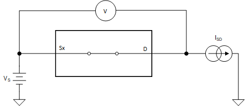 Figure 7. On-Resistance Measurement Setup
 7.2 Off-Leakage Current
Source leakage current is defined as the leakage current flowing into or out of the source pin when the switch is off. This current is denoted by the symbol IS(OFF).
The setup used to measure off-leakage current is shown in Figure 8.
 Figure 8. Off-Leakage Measurement Setup
 7.3 On-Leakage Current
Source on-leakage current is defined as the leakage current flowing into or out of the source pin when the switch is on. This current is denoted by the symbol IS(ON).
Drain on-leakage current is defined as the leakage current flowing into or out of the drain pin when the switch is on. This current is denoted by the symbol ID(ON).
Either the source pin or drain pin is left floating during the measurement. Figure 9 shows the circuit used for measuring the on-leakage current, denoted by IS(ON) or ID(ON).
 Figure 9. On-Leakage Measurement Setup
 7.4 Transition Time
Transition time is defined as the time taken by the output of the device to rise or fall 10% after the logic control signal has risen or fallen past the logic threshold. The 10% transition measurement is utilized to provide the timing of the device. System level timing can then account for the time constant added from the load resistance and load capacitance. Figure 10 shows the setup used to measure transition time, denoted by the symbol tTRANSITION.
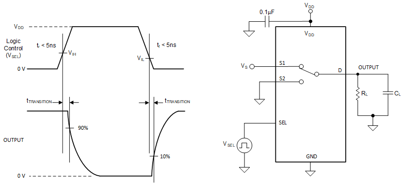 Figure 10. Transition-Time Measurement Setup
 7.5 Break-Before-Make
Break-before-make delay is a safety feature that prevents two inputs from connecting when the device is switching. The output first breaks from the on-state switch before making the connection with the next on-state switch. The time delay between the break and the make is known as break-before-make delay. Figure 11 shows the setup used to measure break-before-make delay, denoted by the symbol tOPEN(BBM).
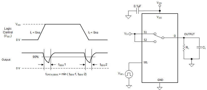 Figure 11. Break-Before-Make Delay Measurement Setup
 7.6 Charge Injection
The TMUX1237 has a transmission-gate topology. Any mismatch in capacitance between the NMOS and PMOS transistors results in a charge injected into the drain or source during the falling or rising edge of the gate signal. The amount of charge injected into the source or drain of the device is known as charge injection, and is denoted by the symbol QC. Figure 12 shows the setup used to measure charge injection from Drain (D) to Source (Sx).
.gif) Figure 12. Charge-Injection Measurement Setup
Figure 12. Charge-Injection Measurement Setup 7.7 Off Isolation
Off isolation is defined as the ratio of the signal at the drain pin (D) of the device when a signal is applied to the source pin (Sx) of an off-channel. Figure 13 shows the setup used to measure, and the equation used to calculate off isolation.
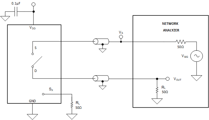 Figure 13. Off Isolation Measurement Setup
7.8 Crosstalk
Crosstalk is defined as the ratio of the signal at the drain pin (D) of a different channel, when a signal is applied at the source pin (Sx) of an on-channel. Figure 14 shows the setup used to measure, and the equation used to calculate crosstalk.
 Figure 14. Crosstalk Measurement Setup
7.9 Bandwidth
Bandwidth is defined as the range of frequencies that are attenuated by less than 3 dB when the input is applied to the source pin (Sx) of an on-channel, and the output is measured at the drain pin (D) of the device. Figure 15 shows the setup used to measure bandwidth.
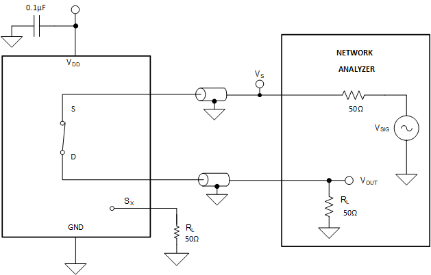 Figure 15. Bandwidth Measurement Setup
 8 Detailed Description
8.1 Overview
The TMUX1237 is an 2:1 (SPDT), 1-channel switch where the input is controlled with a single select (SEL) control pin.
8.2 Functional Block Diagram
 Figure 16. TMUX1237 Functional Block Diagram
 8.3 Feature Description
8.3.1 Bidirectional Operation
The TMUX1237 conducts equally well from source (Sx) to drain (D) or from drain (D) to source (Sx). The device has very similar characteristics in both directions and supports both analog and digital signals.
8.3.2 Rail to Rail Operation
The valid signal path input/output voltage for TMUX1237 ranges from GND to VDD.
8.3.3 1.8 V Logic Compatible Inputs
The TMUX1237 has 1.8-V logic compatible control for the logic control input (SEL). The logic input threshold scales with supply but still provides 1.8-V logic control when operating at 5.5 V supply voltage. 1.8-V logic level inputs allow the TMUX1237 to interface with processors that have lower logic I/O rails and eliminates the need for an external translator, which saves both space and BOM cost. For more information on 1.8 V logic implementations refer to Simplifying Design with 1.8 V logic Muxes and Switches