SCDS399 August 2019 TMUX1247
PRODUCTION DATA.
- 1 Features
- 2 Applications
- 3 Description
- 4 Revision History
- 5 Pin Configuration and Functions
-
6 Specifications
- 6.1 Absolute Maximum Ratings
- 6.2 ESD Ratings
- 6.3 Recommended Operating Conditions
- 6.4 Thermal Information
- 6.5 Electrical Characteristics (VDD = 5 V ±10 %), GND = 0 V unless otherwise specified.
- 6.6 Electrical Characteristics (VDD = 3.3 V ±10 %), GND = 0 V unless otherwise specified.
- 6.7 Electrical Characteristics (VDD = 1.8 V ±10 %), GND = 0 V unless otherwise specified.
- 6.8 Electrical Characteristics (VDD = 1.2 V ±10 %), GND = 0 V unless otherwise specified.
- 6.9 Typical Characteristics
- 7 Parameter Measurement Information
- 8 Detailed Description
- 9 Application and Implementation
- 10Power Supply Recommendations
- 11Layout
- 12Device and Documentation Support
- 13Mechanical, Packaging, and Orderable Information
Package Options
Mechanical Data (Package|Pins)
- DCK|6
Thermal pad, mechanical data (Package|Pins)
Orderable Information
9.2.1 Input Control for Power Amplifier
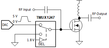
One application of the TMUX1247 is for input control of a power amplifier. Utilizing a switch allows a system to control when the DAC is connected to the power amplifier, and can stop biasing the power amplifier by switching the gate to GND. Figure 17 shows the TMUX1247 configured for control of the power amplifier.
 Figure 17. Input Control of Power Amplifier